Kyocera FS-1050 Service Manual - Page 85
Power supply board, Power supply board circuit block diagram
 |
View all Kyocera FS-1050 manuals
Add to My Manuals
Save this manual to your list of manuals |
Page 85 highlights
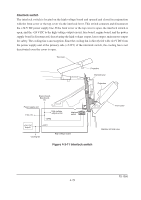
(3) Power supply board The power supply board provides the AC power input and DC power and outputs. The high voltage bias generator circuit is mounted on a separate board. A simplified schematic diagram is shown below. AC input Power Current switch fuse (SW1) (F1) Noise filter circuit Power supply unit Exit sensor Transformer (T1) 24 V DC rectifier/ smoothing circuit 24 V DC shutoff circuit Heater lamp Thermal cutout FET (Q1) Switching/ Over current detection circuit 5 V DC rectifier/ smoothing circuit Photocoupler (PC1) Over voltage detection circuit Triac (TRC1) Photocoupler (PC3) Transistor (Q8) Zero cross signal detection circuit PhotoTriac (PC2) EXITN +24 V COM SLEEP FAN Cooling fan +24 V COM +5 V PGND, SGND THERM Thermistor +24 V ZCROSS HEAT Figure 4-3-8 Power supply board circuit block diagram FS-1050 4-26
-
 1
1 -
2
-
3
-
4
-
5
-
6
-
7
-
8
-
9
-
10
-
11
-
12
-
13
-
14
-
15
-
16
-
17
-
18
-
19
-
20
-
21
-
22
-
23
-
24
-
25
-
26
-
27
-
28
-
29
-
30
-
31
-
32
-
33
-
34
-
35
-
36
-
37
-
38
-
39
-
40
-
41
-
42
-
43
-
44
-
45
-
46
-
47
-
48
-
49
-
50
-
51
-
52
-
53
-
54
-
55
-
56
-
57
-
58
-
59
-
60
-
61
-
62
-
63
-
64
-
65
-
66
-
67
-
68
-
69
-
70
-
71
-
72
-
73
-
74
-
75
-
76
-
77
-
78
-
79
-
 80
80 -
 81
81 -
 82
82 -
 83
83 -
 84
84 -
 85
85 -
 86
86 -
 87
87 -
 88
88 -
 89
89 -
 90
90 -
91
-
92
-
93
-
94
-
95
-
96
-
97
-
98
-
99
-
100
-
101
-
102
-
103
-
104
-
105
-
106
-
107
-
108
-
109
-
110
-
111
-
112
-
113
-
114
-
115
-
116
-
117
-
118
-
119
-
120
-
121
-
122
-
123
-
124
-
125
-
126
-
127
-
128
-
129
-
130
-
131
-
132
-
133
-
134
-
135
-
136
-
137
-
138
-
139
-
140
-
141
-
142
-
143
-
144
-
145
-
146
-
147
-
148
-
149
-
150
-
151
-
152
-
153
-
154
-
155
-
156
-
157
-
158
-
159
-
160
-
161
-
162
-
163
-
164
-
165
-
166
-
167
-
168
-
169
-
170
-
171
-
172
-
173
-
174
-
175
-
176
-
177
 |
 |
