HP rp8420 HP 9000 rp8420 Server - User Service Guide, Fifth Edition - Page 31
System Backplane to PCI-X Backplane Connectivity, Clocks and Reset, I/O Subsystem
 |
View all HP rp8420 manuals
Add to My Manuals
Save this manual to your list of manuals |
Page 31 highlights
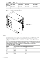
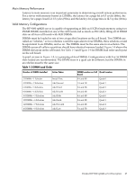
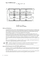
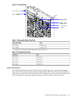
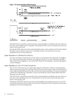
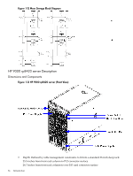
System Backplane to PCI-X Backplane Connectivity The PCI-X backplane uses two connectors for the SBA link bus and two connectors for the high-speed data signals and the manageability signals. SBA link bus signals are routed through the system backplane to the CC on each corresponding cell board. The high-speed data signals are routed from the SBA chips on the PCI-X backplane to the two LBA PCI bus controllers on the system backplane. Clocks and Reset The system backplane contains reset and clock circuitry that propagates through the whole system. The system backplane central clocks drive all major chip set clocks. I/O Subsystem The cell board to the PCI-X board path runs from the CC to the SBA, from the SBA to the ropes, from the ropes to the LBA, and from the LBA to the PCI slots seen in Figure 1-11. The CC on cell board 0 and cell board 1 communicates through an SBA over the SBA link. The SBA link consists of both an inbound and an outbound link with an effective bandwidth of approximately 1 GB/sec. The SBA converts the SBA link protocol into "ropes." A rope is defined as a high-speed, point-to-point data bus. The SBA can support up to 16 of these high-speed, bi-directional rope links for a total aggregate bandwidth of approximately 4 GB/sec. Each LBA acts as a bus bridge, supporting either one or two ropes and capable of driving 33 MHz or 66 MHz for PCI cards. The LBAs can also drive at 66 MHz or 133 MHz for PCI-X cards. When cell board 2 and cell board 3 are present, the cell boards attach to their own associated SBA and LBA chips on the PCI-X board in the Server Expansion Unit. Detailed HP 9000 rp8420 server Description 31
-
 1
1 -
2
-
3
-
4
-
5
-
6
-
7
-
8
-
9
-
10
-
11
-
12
-
13
-
14
-
15
-
16
-
17
-
18
-
19
-
20
-
21
-
22
-
23
-
24
-
25
-
 26
26 -
 27
27 -
 28
28 -
 29
29 -
 30
30 -
 31
31 -
 32
32 -
 33
33 -
 34
34 -
 35
35 -
 36
36 -
37
-
38
-
39
-
40
-
41
-
42
-
43
-
44
-
45
-
46
-
47
-
48
-
49
-
50
-
51
-
52
-
53
-
54
-
55
-
56
-
57
-
58
-
59
-
60
-
61
-
62
-
63
-
64
-
65
-
66
-
67
-
68
-
69
-
70
-
71
-
72
-
73
-
74
-
75
-
76
-
77
-
78
-
79
-
80
-
81
-
82
-
83
-
84
-
85
-
86
-
87
-
88
-
89
-
90
-
91
-
92
-
93
-
94
-
95
-
96
-
97
-
98
-
99
-
100
-
101
-
102
-
103
-
104
-
105
-
106
-
107
-
108
-
109
-
110
-
111
-
112
-
113
-
114
-
115
-
116
-
117
-
118
-
119
-
120
-
121
-
122
-
123
-
124
-
125
-
126
-
127
-
128
-
129
-
130
-
131
-
132
-
133
-
134
-
135
-
136
-
137
-
138
-
139
-
140
-
141
-
142
-
143
-
144
-
145
-
146
-
147
-
148
-
149
-
150
-
151
-
152
-
153
-
154
-
155
-
156
-
157
-
158
-
159
-
160
-
161
-
162
-
163
-
164
-
165
-
166
-
167
-
168
-
169
-
170
-
171
-
172
-
173
-
174
-
175
-
176
-
177
-
178
-
179
-
180
-
181
-
182
-
183
-
184
-
185
-
186
-
187
-
188
-
189
-
190
-
191
-
192
-
193
-
194
-
195
-
196
-
197
-
198
-
199
-
200
-
201
-
202
-
203
-
204
-
205
-
206
-
207
-
208
-
209
-
210
-
211
-
212
-
213
-
214
-
215
 |
 |
