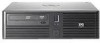
HP Rp5700 HP rp5700 Business System Service Reference Guide, 1st Edition - Page 190
SPI ROM and socket XU19 = socket, U19 = SPI ROM, System ROM and Socket Socket = XU15, ROM = U15
 |
UPC - 884420470731
View all HP Rp5700 manuals
Add to My Manuals
Save this manual to your list of manuals |
Page 190 highlights
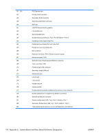
U32 U46 U50 U51 U52 U53 XBT XMM1 XMM2 - XMM5 XU1 XU2 XU15/U15 XU19/U19 Y1 Y2 Y3 Y4 Y5/H5 Second serial port transceiver VRM controller USB front port power switch First USB rear port power switch Second USB rear port power switch Third USB rear port power switch Battery retainer Memory slot. DIMM1 or RIMM1 populated and tested Following memory slots Primary processor socket Secondary processor socket System ROM and Socket (Socket = XU15, ROM = U15) SPI ROM and socket (XU19 = socket, U19 = SPI ROM) Primary (TH) system clock crystal Secondary (SMT) system clock crystal Primary NIC clock crystal Secondary NIC clock crystal RTC clock crystal/tie-down 180 Appendix E System Board and Riser Board Reference Designators ENWW
-
 1
1 -
2
-
3
-
4
-
5
-
6
-
7
-
8
-
9
-
10
-
11
-
12
-
13
-
14
-
15
-
16
-
17
-
18
-
19
-
20
-
21
-
22
-
23
-
24
-
25
-
26
-
27
-
28
-
29
-
30
-
31
-
32
-
33
-
34
-
35
-
36
-
37
-
38
-
39
-
40
-
41
-
42
-
43
-
44
-
45
-
46
-
47
-
48
-
49
-
50
-
51
-
52
-
53
-
54
-
55
-
56
-
57
-
58
-
59
-
60
-
61
-
62
-
63
-
64
-
65
-
66
-
67
-
68
-
69
-
70
-
71
-
72
-
73
-
74
-
75
-
76
-
77
-
78
-
79
-
80
-
81
-
82
-
83
-
84
-
85
-
86
-
87
-
88
-
89
-
90
-
91
-
92
-
93
-
94
-
95
-
96
-
97
-
98
-
99
-
100
-
101
-
102
-
103
-
104
-
105
-
106
-
107
-
108
-
109
-
110
-
111
-
112
-
113
-
114
-
115
-
116
-
117
-
118
-
119
-
120
-
121
-
122
-
123
-
124
-
125
-
126
-
127
-
128
-
129
-
130
-
131
-
132
-
133
-
134
-
135
-
136
-
137
-
138
-
139
-
140
-
141
-
142
-
143
-
144
-
145
-
146
-
147
-
148
-
149
-
150
-
151
-
152
-
153
-
154
-
155
-
156
-
157
-
158
-
159
-
160
-
161
-
162
-
163
-
164
-
165
-
166
-
167
-
168
-
169
-
170
-
171
-
172
-
173
-
174
-
175
-
176
-
177
-
178
-
179
-
180
-
181
-
182
-
183
-
184
-
 185
185 -
 186
186 -
 187
187 -
 188
188 -
 189
189 -
 190
190 -
 191
191 -
 192
192 -
 193
193 -
 194
194 -
 195
195 -
196
 |
 |

U32
U46
U50
U51
U52
Second serial port transceiver
VRM controller
USB front port power switch
First USB rear port power switch
Second USB rear port power switch
U53
XBT
XMM1
XMM2 - XMM5
XU1
Third USB rear port power switch
Battery retainer
Memory slot. DIMM1 or RIMM1 populated and tested
Following memory slots
Primary processor socket
XU2
XU15/U15
XU19/U19
Y1
Y2
Secondary processor socket
System ROM and Socket (Socket = XU15, ROM = U15)
SPI ROM and socket (XU19 = socket, U19 = SPI ROM)
Primary (TH) system clock crystal
Secondary (SMT) system clock crystal
Y3
Y4
Y5/H5
Primary NIC clock crystal
Secondary NIC clock crystal
RTC clock crystal/tie-down
180
Appendix E
System Board and Riser Board Reference Designators
ENWW