Intel BX80601920 Data Sheet - Page 13
Electrical Specifications
 |
UPC - 735858204736
View all Intel BX80601920 manuals
Add to My Manuals
Save this manual to your list of manuals |
Page 13 highlights
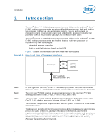
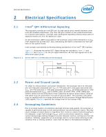
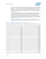
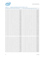
Electrical Specifications 2 Electrical Specifications 2.1 Intel® QPI Differential Signaling The processor provides an Intel QPI port for high speed serial transfer between other Intel QPI-enabled components. The Intel QPI port consists of two unidirectional links (for transmit and receive). Intel QPI uses a differential signalling scheme where pairs of opposite-polarity (D_P, D_N) signals are used. On-die termination (ODT) is provided on the processor silicon and termination is to VSS. Intel chipsets also provide ODT; thus, eliminating the need to terminate the Intel QPI links on the system board. Intel strongly recommends performing analog simulations of the Intel® QPI interface. Figure 2-1 illustrates the active ODT. Signal listings are included in Table 2-3 and Table 2-4. See Chapter 5 for the pin signal definitions. All Intel QPI signals are in the differential signal group. Figure 2-1. Active ODT for a Differential Link Example TX RTT RTT Signal Signal RX RTT RTT 2.2 2.3 Power and Ground Lands For clean on-chip processor core power distribution, the processor has 210 VCC pads and 119 VSS pads associated with VCC; 8 VTTA pads and 5 VSS pads associated with VTTA; 28 VTTD pads and 17 VSS pads associated with VTTD, 28 VDDQ pads and 17 VSS pads associated with VDDQ; and 3 VCCPLL pads. All VCCP, VTTA, VTTD, VDDQ and VCCPLL lands must be connected to their respective processor power planes, while all VSS lands must be connected to the system ground plane. The processor VCC lands must be supplied with the voltage determined by the processor Voltage IDentification (VID) signals. Table 2-1 specifies the voltage level for the various VIDs. Decoupling Guidelines Due to its large number of transistors and high internal clock speeds, the processor is capable of generating large current swings between low and full power states. This may cause voltages on power planes to sag below their minimum values if bulk decoupling is not adequate. Larger bulk storage (CBULK), such as electrolytic capacitors, supply current during longer lasting changes in current demand; such as, coming out of an idle condition. Similarly, capacitors act as a storage well for current when entering an idle condition from a running condition. Care must be taken in the baseboard design to Datasheet 13
-
 1
1 -
2
-
3
-
4
-
5
-
6
-
7
-
 8
8 -
 9
9 -
 10
10 -
 11
11 -
 12
12 -
 13
13 -
 14
14 -
 15
15 -
 16
16 -
 17
17 -
 18
18 -
19
-
20
-
21
-
22
-
23
-
24
-
25
-
26
-
27
-
28
-
29
-
30
-
31
-
32
-
33
-
34
-
35
-
36
-
37
-
38
-
39
-
40
-
41
-
42
-
43
-
44
-
45
-
46
-
47
-
48
-
49
-
50
-
51
-
52
-
53
-
54
-
55
-
56
-
57
-
58
-
59
-
60
-
61
-
62
-
63
-
64
-
65
-
66
-
67
-
68
-
69
-
70
-
71
-
72
-
73
-
74
-
75
-
76
-
77
-
78
-
79
-
80
-
81
-
82
-
83
-
84
-
85
-
86
-
87
-
88
-
89
-
90
-
91
-
92
-
93
-
94
-
95
-
96
 |
 |