Intel BX80601920 Data Sheet - Page 21
Absolute Maximum and Minimum Ratings
 |
UPC - 735858204736
View all Intel BX80601920 manuals
Add to My Manuals
Save this manual to your list of manuals |
Page 21 highlights
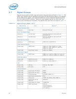
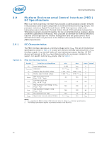
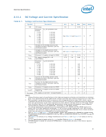
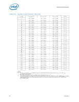
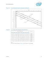
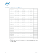
Electrical Specifications 2.9.2 Input Device Hysteresis The input buffers in both client and host models must use a Schmitt-triggered input design for improved noise immunity. Use Figure 2-2 as a guide for input buffer design. Figure 2-2. Input Device Hysteresis VTTD Maximum VP Minimum VP Maximum VN Minimum VN PECI Ground PECI High Range PECI Low Range Minimum Valid Input Hysteresis Signal Range 2.10 Absolute Maximum and Minimum Ratings Table 2-6 specifies absolute maximum and minimum ratings, which lie outside the functional limits of the processor. Only within specified operation limits can functionality and long-term reliability be expected. At conditions outside functional operation condition limits, but within absolute maximum and minimum ratings, neither functionality nor long-term reliability can be expected. If a device is returned to conditions within functional operation limits after having been subjected to conditions outside these limits, but within the absolute maximum and minimum ratings, the device may be functional, but with its lifetime degraded depending on exposure to conditions exceeding the functional operation condition limits. At conditions exceeding absolute maximum and minimum ratings, neither functionality nor long-term reliability can be expected. Moreover, if a device is subjected to these conditions for any length of time then, when returned to conditions within the functional operating condition limits, it will either not function or its reliability will be severely degraded. Although the processor contains protective circuitry to resist damage from ElectroStatic Discharge (ESD), precautions should always be taken to avoid high static voltages or electric fields. Datasheet 21
-
 1
1 -
2
-
3
-
4
-
5
-
6
-
7
-
8
-
9
-
10
-
11
-
12
-
13
-
14
-
15
-
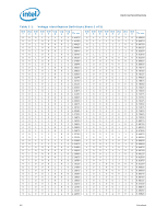 16
16 -
 17
17 -
 18
18 -
 19
19 -
 20
20 -
 21
21 -
 22
22 -
 23
23 -
 24
24 -
 25
25 -
 26
26 -
27
-
28
-
29
-
30
-
31
-
32
-
33
-
34
-
35
-
36
-
37
-
38
-
39
-
40
-
41
-
42
-
43
-
44
-
45
-
46
-
47
-
48
-
49
-
50
-
51
-
52
-
53
-
54
-
55
-
56
-
57
-
58
-
59
-
60
-
61
-
62
-
63
-
64
-
65
-
66
-
67
-
68
-
69
-
70
-
71
-
72
-
73
-
74
-
75
-
76
-
77
-
78
-
79
-
80
-
81
-
82
-
83
-
84
-
85
-
86
-
87
-
88
-
89
-
90
-
91
-
92
-
93
-
94
-
95
-
96
 |
 |
