Intel BX80601920 Data Sheet - Page 22
Processor DC Specifications
 |
UPC - 735858204736
View all Intel BX80601920 manuals
Add to My Manuals
Save this manual to your list of manuals |
Page 22 highlights
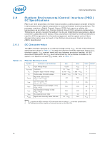
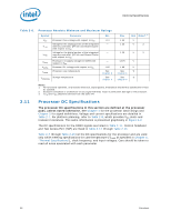
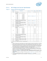
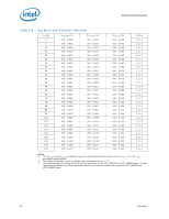
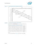
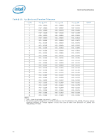
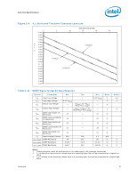
Electrical Specifications . Table 2-6. Processor Absolute Minimum and Maximum Ratings Symbol VCC VTTA VTTD VDDQ VCCPLL TCASE TSTORAGE Parameter Processor Core voltage with respect to VSS Voltage for the analog portion of the integrated memory controller, QPI link and Shared Cache with respect to VSS Voltage for the digital portion of the integrated memory controller, QPI link and Shared Cache with respect to VSS Processor I/O supply voltage for DDR3 with respect to VSS Processor PLL voltage with respect to VSS Processor case temperature Storage temperature Min -0.3 - - - 1.65 See Chapter 6 See Chapter 6 Max 1.55 1.35 Unit Notes1, 2 V V 3 1.35 V 3 1.875 V 1.89 V See C Chapter 6 See C Chapter 6 Notes: 1. For functional operation, all processor electrical, signal quality, mechanical and thermal specifications must be satisfied. 2. Excessive overshoot or undershoot on any signal will likely result in permanent damage to the processor. 3. VTTA and VTTD should be derived from the same VR. 2.11 Processor DC Specifications The processor DC specifications in this section are defined at the processor pads, unless noted otherwise. See Chapter 4 for the processor land listings and Chapter 5 for signal definitions. Voltage and current specifications are detailed in Table 2-7. For platform planning, refer to Table 2-8, which provides VCC static and transient tolerances. This same information is presented graphically in Figure 2-3. The DC specifications for the DDR3 signals are listed in Table 2-11. Control Sideband and Test Access Port (TAP) are listed in Table 2-12 through Table 2-15. Table 2-7 through Table 2-15 list the DC specifications for the processor and are valid only while meeting specifications for case temperature (TCASE as specified in Chapter 6, "Thermal Specifications"), clock frequency, and input voltages. Care should be taken to read all notes associated with each parameter. 22 Datasheet
-
 1
1 -
2
-
3
-
4
-
5
-
6
-
7
-
8
-
9
-
10
-
11
-
12
-
13
-
14
-
15
-
16
-
 17
17 -
 18
18 -
 19
19 -
 20
20 -
 21
21 -
 22
22 -
 23
23 -
 24
24 -
 25
25 -
 26
26 -
 27
27 -
28
-
29
-
30
-
31
-
32
-
33
-
34
-
35
-
36
-
37
-
38
-
39
-
40
-
41
-
42
-
43
-
44
-
45
-
46
-
47
-
48
-
49
-
50
-
51
-
52
-
53
-
54
-
55
-
56
-
57
-
58
-
59
-
60
-
61
-
62
-
63
-
64
-
65
-
66
-
67
-
68
-
69
-
70
-
71
-
72
-
73
-
74
-
75
-
76
-
77
-
78
-
79
-
80
-
81
-
82
-
83
-
84
-
85
-
86
-
87
-
88
-
89
-
90
-
91
-
92
-
93
-
94
-
95
-
96
 |
 |
