Intel BX80601920 Data Sheet - Page 23
DC Voltage and Current Specification - core i7 920
 |
UPC - 735858204736
View all Intel BX80601920 manuals
Add to My Manuals
Save this manual to your list of manuals |
Page 23 highlights
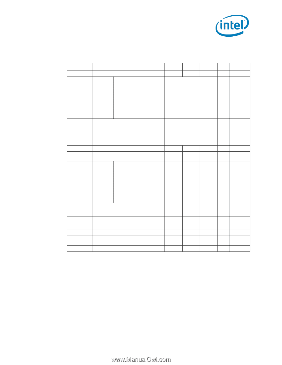
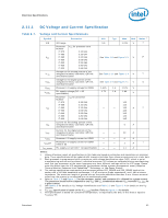
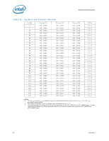
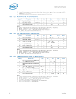
Electrical Specifications 2.11.1 DC Voltage and Current Specification Table 2-7. Voltage and Current Specifications Symbol Parameter Min Typ Max Unit Notes 1 VID VID range 0.8 - 1.375 V 2 Processor VCC for processor core Number i7-975 3.33 GHz i7-965 3.20 GHz VCC i7-960 i7-950 3.20 GHz 3.06 GHz i7-940 2.93 GHz i7-930 2.80 GHz i7-920 2.66 GHz See Table 2-8 and Figure 2-3 V 3,4 Voltage for the analog portion of the VTTA integrated memory controller, QPI link See Table 2-10 and Figure 2-4 V 5 and Shared Cache Voltage for the digital portion of the VTTD integrated memory controller, QPI link See Table 2-9 and Figure 2-4 V 5 and Shared Cache VDDQ VCCPLL Processor I/O supply voltage for DDR3 PLL supply voltage (DC + AC specification) 1.425 1.5 1.575 V 1.71 1.8 1.89 V Processor ICC for processor Number i7-975 3.33 GHz i7-965 3.20 GHz ICC i7-960 i7-950 3.20 GHz 3.06 GHz i7-940 2.93 GHz i7-930 2.80 GHz i7-920 2.66 GHz 145 145 - - 145 A 6 145 145 145 145 Current for the analog portion of the ITTA integrated memory controller, QPI link and Shared Cache - - 5 A ITTD Current for the digital portion of the integrated memory controller, QPI link and Shared Cache - - 23 A IDDQ IDDQS3 Processor I/O supply current for DDR3 Processor I/O supply current for DDR3 while in S3 - - - - 6 A 1 A 7 ICC_VCCPLL PLL supply current (DC + AC specification) - - 1.1 A Notes: 1. Unless otherwise noted, all specifications in this table are based on estimates and simulations or empirical data. These specifications will be updated with characterized data from silicon measurements at a later date 2. Each processor is programmed with a maximum valid voltage identification value (VID), which is set at manufacturing and can not be altered. Individual maximum VID values are calibrated during manufacturing such that two processors at the same frequency may have different settings within the VID range. Please nThoteermthailsMdoifnfeitrosr,frEonmhatnhceeVdIDInteeml SplpoeyeeddSbteypt®heTepcrohcneoslosogry,dourriLnogwaPpoowweerrSmtaatneasg).ement event (Adaptive 3. The voltage specification requirements are measured across VCC_SENSE and VSS_SENSE lands at the socket with a 100 MHz bandwidth oscilloscope, 1.5 pF maximum probe capacitance, and 1 M minimum impedance. The maximum length of ground wire on the probe should be less than 5 mm. Ensure external noise from the system is not coupled into the oscilloscope probe. 4. Refer to Table 2-8 and Figure 2-3 for the minimum, typical, and maximum VCC allowed for a given current. The processor should not be subjected to any VCC and ICC combination wherein VCC exceeds VCC_MAX for a given current. 5. See Table 2-9 for details on VTT Voltage Identification and Table 2-9 and Figure 2-4 for details on the VTT Loadline. 6. 7. ITChCis_MsApXecsifpiceactiifoicnatiisobnaissebdaosnedaopnrothceesVsoCrCt_eMmAXpeloraatdulrinee, .aRs erefeprotroteFdigbuyreth2e-3DTfoSr,doeftaleilsss. than or equal to TCONTROL-25. Datasheet 23
-
 1
1 -
2
-
3
-
4
-
5
-
6
-
7
-
8
-
9
-
10
-
11
-
12
-
13
-
14
-
15
-
16
-
17
-
 18
18 -
 19
19 -
 20
20 -
 21
21 -
 22
22 -
 23
23 -
 24
24 -
 25
25 -
 26
26 -
 27
27 -
 28
28 -
29
-
30
-
31
-
32
-
33
-
34
-
35
-
36
-
37
-
38
-
39
-
40
-
41
-
42
-
43
-
44
-
45
-
46
-
47
-
48
-
49
-
50
-
51
-
52
-
53
-
54
-
55
-
56
-
57
-
58
-
59
-
60
-
61
-
62
-
63
-
64
-
65
-
66
-
67
-
68
-
69
-
70
-
71
-
72
-
73
-
74
-
75
-
76
-
77
-
78
-
79
-
80
-
81
-
82
-
83
-
84
-
85
-
86
-
87
-
88
-
89
-
90
-
91
-
92
-
93
-
94
-
95
-
96
 |
 |