Intel BX80601920 Data Sheet - Page 67
Signal Descriptions
 |
UPC - 735858204736
View all Intel BX80601920 manuals
Add to My Manuals
Save this manual to your list of manuals |
Page 67 highlights
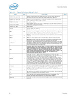
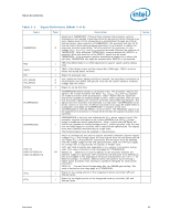
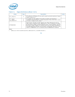
Signal Descriptions 5 Signal Descriptions This chapter provides a description of each processor signal. Table 5-1. Signal Definitions (Sheet 1 of 4) Name BCLK_DN BCLK_DP BCLK_ITP_DN BCLK_ITP_DP BPM#[7:0] CAT_ERR# COMP0 QPI_CLKRX_DN QPI_CLKRX_DP QPI_CLKTX_DN QPI_CLKTX_DP QPI_CMP[0] QPI_DRX_DN[19:0] QPI_DRX_DP[19:0] QPI_DTX_DN[19:0] QPI_DTX_DP[19:0] DBR# DDR_COMP[2:0] DDR_VREF DDR{0/1/2}_BA[2:0] DDR{0/1/2}_CAS# DDR{0/1/2}_CKE[3:0] DDR{0/1/2}_CLK_N[2:0] DDR{0/1/2}_CLK_P[2:0] DDR{0/1/2}_CS[1:0]# DDR{0/1/2}_CS[5:4]# DDR{0/1/2}_DQ[63:0] DDR{0/1/2}_DQS_N[7:0] DDR{0/1/2}_DQS_P[7:0] Type Description I Differential bus clock input to the processor. Notes O Buffered differential bus clock pair to ITP. BPM#[7:0] are breakpoint and performance monitor signals. They are outputs from the processor that indicate the status of breakpoints and programmable I/O counters used for monitoring processor performance. BPM#[7:0] should be connected in a wired OR topology between all packages on a platform. The end points for the wired OR connections must be terminated. CAT_ERR# indicates that the system has experienced a catastrophic error and cannot continue to operate. The processor will set this for non-recoverable I/O machine check errors and other internal unrecoverable error. Since this is an I/ O pin, external agents are allowed to assert this pin which will cause the processor to take a machine check exception. I Impedance compensation must be terminated on the system board using a precision resistor. I I Intel QPI received clock is the input clock that corresponds to the received data. O O Intel QPI forwarded clock sent with the outbound data. I Must be terminated on the system board using a precision resistor. I I QPI_DRX_DN[19:0] and QPI_DRX_DP[19:0] comprise the differential receive data for the QPI port. The inbound 20 lanes are connected to another component's outbound direction. O O QPI_DTX_DN[19:0] and QPIQPI_DTX_DP[19:0] comprise the differential transmit data for the QPI port. The outbound 20 lanes are connected to another component's inbound direction. DBR# is used only in systems where no debug port is implemented on the I system board. DBR# is used by a debug port interposer so that an in-target probe can drive system reset. If a debug port is implemented in the system, DBR# is a no connect in the system. DBR# is not a processor signal. I Must be terminated on the system board using precision resistors. I Voltage reference for DDR3 O Defines the bank which is the destination for the current Activate, Read, Write, or Precharge command. 1 O Column Address Strobe. O Clock Enable. O Differential clocks to the DIMM. All command and control signals are valid on the rising edge of clock. O Each signal selects one rank as the target of the command and address. I/O DDR3 Data bits. Differential pair, Data Strobe x8. Differential strobes latch data for each DRAM. I/O Different numbers of strobes are used depending on whether the connected DRAMs are x4 or x8. Driven with edges in center of data, receive edges are aligned with data edges. Datasheet 67
-
 1
1 -
2
-
3
-
4
-
5
-
6
-
7
-
8
-
9
-
10
-
11
-
12
-
13
-
14
-
15
-
16
-
17
-
18
-
19
-
20
-
21
-
22
-
23
-
24
-
25
-
26
-
27
-
28
-
29
-
30
-
31
-
32
-
33
-
34
-
35
-
36
-
37
-
38
-
39
-
40
-
41
-
42
-
43
-
44
-
45
-
46
-
47
-
48
-
49
-
50
-
51
-
52
-
53
-
54
-
55
-
56
-
57
-
58
-
59
-
60
-
61
-
 62
62 -
 63
63 -
 64
64 -
 65
65 -
 66
66 -
 67
67 -
 68
68 -
 69
69 -
 70
70 -
 71
71 -
 72
72 -
73
-
74
-
75
-
76
-
77
-
78
-
79
-
80
-
81
-
82
-
83
-
84
-
85
-
86
-
87
-
88
-
89
-
90
-
91
-
92
-
93
-
94
-
95
-
96
 |
 |
