Intel BX80601920 Data Sheet - Page 18
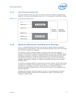
Signal Groups
 |
UPC - 735858204736
View all Intel BX80601920 manuals
Add to My Manuals
Save this manual to your list of manuals |
Page 18 highlights
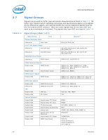
Electrical Specifications 2.7 Signal Groups Signals are grouped by buffer type and similar characteristics as listed in Table 2-3. The buffer type indicates which signaling technology and specifications apply to the signals. All the differential signals, and selected DDR3 and Control Sideband signals have OnDie Termination (ODT) resistors. There are some signals that do not have ODT and need to be terminated on the board. The signals that have ODT are listed in Table 2-4. Table 2-3. Signal Groups (Sheet 1 of 2) Signal Group Type System Reference Clock Differential Clock Input Intel® QPI Signal Groups Differential Intel QPI Input Differential Intel QPI Output DDR3 Reference Clocks Differential DDR3 Output DDR3 Command Signals Single ended CMOS Output Single ended Asynchronous Output DDR3 Control Signals Single ended CMOS Output DDR3 Data Signals Single ended Differential TAP Single ended Single ended Control Sideband Single ended Single ended Single ended Single Ended Single Ended Single ended Single ended Single ended CMOS Bi-directional CMOS Bi-directional TAP Input GTL Output Asynchronous GTL Output Asynchronous GTL Input GTL Bi-directional Asynchronous Bi-directional Analog Input Asynchronous GTL Bidirectional Asynchronous GTL Output CMOS Input/Output Signals1,2 BCLK_DP, BCLK_DN QPI_DRX_D[N/P][19:0], QPI_CLKRX_DP, QPI_CLKRX_DN QPI_DTX_D[N/P][19:0], QPI_CLKTX_DP, QPI_CLKTX_DN DDR{0/1/2}_CLK[D/P][3:0] DDR{0/1/2}_RAS#, DDR{0/1/2}_CAS#, DDR{0/1/2}_WE#, DDR{0/1/2}_MA[15:0], DDR{0/1/2}_BA[2:0] DDR{0/1/2}_RESET# DDR{0/1/2}_CS#[5:4], DDR{0/1/2}_CS#[1:0], DDR{0/1/2}_ODT[3:0], DDR{0/1/2}_CKE[3:0] DDR{0/1/2}_DQ[63:0] DDR{0/1/2}_DQS_[N/P][7:0] TCK, TDI, TMS, TRST# TDO PRDY# PREQ# CAT_ERR#, BPM#[7:0] PECI COMP0, QPI_CMP[0], DDR_COMP[2:0] PROCHOT# THERMTRIP# VID[7:6] VID[5:3]/CSC[2:0] VID[2:0]/MSID[2:0] VTT_VID[4:2] 18 Datasheet
-
 1
1 -
2
-
3
-
4
-
5
-
6
-
7
-
8
-
9
-
10
-
11
-
12
-
 13
13 -
 14
14 -
 15
15 -
 16
16 -
 17
17 -
 18
18 -
 19
19 -
 20
20 -
 21
21 -
 22
22 -
 23
23 -
24
-
25
-
26
-
27
-
28
-
29
-
30
-
31
-
32
-
33
-
34
-
35
-
36
-
37
-
38
-
39
-
40
-
41
-
42
-
43
-
44
-
45
-
46
-
47
-
48
-
49
-
50
-
51
-
52
-
53
-
54
-
55
-
56
-
57
-
58
-
59
-
60
-
61
-
62
-
63
-
64
-
65
-
66
-
67
-
68
-
69
-
70
-
71
-
72
-
73
-
74
-
75
-
76
-
77
-
78
-
79
-
80
-
81
-
82
-
83
-
84
-
85
-
86
-
87
-
88
-
89
-
90
-
91
-
92
-
93
-
94
-
95
-
96
 |
 |
