Intel BX80601920 Data Sheet - Page 27
Symbol, Parameter, Units, Notes
 |
UPC - 735858204736
View all Intel BX80601920 manuals
Add to My Manuals
Save this manual to your list of manuals |
Page 27 highlights
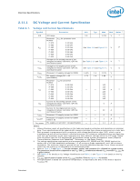
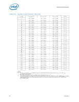
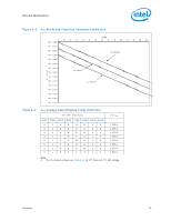
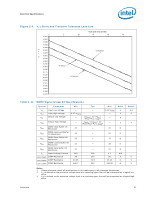
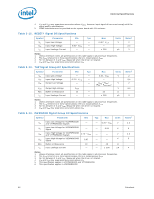
Electrical Specifications Figure 2-4. VTT Static and Transient Tolerance Load Line Itt [A] (sum of Itta and Ittd) 0 0.0500 5 10 15 20 25 0.0375 0.0250 0.0125 0.0000 V -0.0125 t t -0.0250 -0.0375 V -0.0500 Vtt Maximum -0.0625 -0.0750 -0.0875 Vtt Typical -0.1000 -0.1125 -0.1250 -0.1375 Vtt Minimum -0.1500 -0.1625 -0.1750 -0.1875 -0.2000 -0.2125 Table 2-11. DDR3 Signal Group DC Specifications Symbol Parameter Min Typ Max VIL Input Low Voltage VIH Input High Voltage VOL Output Low Voltage VOH Output High Voltage RON DDR3 Clock Buffer On Resistance RON DDR3 Command Buffer On Resistance RON DDR3 Reset Buffer On Resistance RON DDR3 Control Buffer On Resistance RON DDR3 Data Buffer On Resistance ILI DDR_COMP0 DDR_COMP1 DDR_COMP2 Input Leakage Current COMP Resistance COMP Resistance COMP Resistance - 0.57*VDDQ - - - - ((VRDODNQ+R/ V2T)T*_T(ERROMN))/ (RVODND/Q(R-ON((+VRDVDTQT_/TE2R)M*)) 0.43*VDDQ - - - 21 - 31 16 - 24 25 - 75 21 - 31 21 N/A 99 24.65 128.7 - N/A 100 24.9 130 31 ± 1 101 25.15 131.30 Units V V V V mA Notes1 2,4 3 4 5 5 5 Notes: 1. Unless otherwise noted, all specifications in this table apply to all processor frequencies. 2. VIL is defined as the maximum voltage level at a receiving agent that will be interpreted as a logical low value. 3. VIH is defined as the minimum voltage level at a receiving agent that will be interpreted as a logical high value. Datasheet 27
-
 1
1 -
2
-
3
-
4
-
5
-
6
-
7
-
8
-
9
-
10
-
11
-
12
-
13
-
14
-
15
-
16
-
17
-
18
-
19
-
20
-
21
-
 22
22 -
 23
23 -
 24
24 -
 25
25 -
 26
26 -
 27
27 -
 28
28 -
 29
29 -
 30
30 -
 31
31 -
 32
32 -
33
-
34
-
35
-
36
-
37
-
38
-
39
-
40
-
41
-
42
-
43
-
44
-
45
-
46
-
47
-
48
-
49
-
50
-
51
-
52
-
53
-
54
-
55
-
56
-
57
-
58
-
59
-
60
-
61
-
62
-
63
-
64
-
65
-
66
-
67
-
68
-
69
-
70
-
71
-
72
-
73
-
74
-
75
-
76
-
77
-
78
-
79
-
80
-
81
-
82
-
83
-
84
-
85
-
86
-
87
-
88
-
89
-
90
-
91
-
92
-
93
-
94
-
95
-
96
 |
 |
