Intel BX80601920 Data Sheet - Page 14
Processor Clocking BCLK_DP, BCLK_DN, Voltage Identification VID
 |
UPC - 735858204736
View all Intel BX80601920 manuals
Add to My Manuals
Save this manual to your list of manuals |
Page 14 highlights
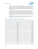
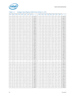
Electrical Specifications 2.3.1 2.4 2.4.1 2.5 ensure that the voltage provided to the processor remains within the specifications listed in Table 2-7. Failure to do so can result in timing violations or reduced lifetime of the processor. VCC, VTTA, VTTD, VDDQ Decoupling Voltage regulator solutions need to provide bulk capacitance and the baseboard designer must assure a low interconnect resistance from the regulator to the LGA1366 socket. Bulk decoupling must be provided on the baseboard to handle large current swings. The power delivery solution must insure the voltage and current specifications are met (as defined in Table 2-7). Processor Clocking (BCLK_DP, BCLK_DN) The processor core, Intel QPI, and integrated memory controller frequencies are generated from BCLK_DP and BCLK_DN. Unlike previous processors based on front side bus architecture, there is no direct link between core frequency and Intel QPI link frequency (such as, no core frequency to Intel QPI multiplier). The processor maximum core frequency, Intel QPI link frequency and integrated memory controller frequency, are set during manufacturing. It is possible to override the processor core frequency setting using software. This permits operation at lower core frequencies than the factory set maximum core frequency. The processor's maximum non-turbo core frequency is configured during power-on reset by using values stored internally during manufacturing. The stored value sets the highest core multiplier at which the particular processor can operate. If lower max nonturbo speeds are desired, the appropriate ratio can be configured using the CLOCK_FLEX_MAX MSR. The processor uses differential clocks (BCLK_DP, BCLK_DN). Clock multiplying within the processor is provided by the internal phase locked loop (PLL), which requires a constant frequency BCLK_DP, BCLK_DN input, with exceptions for spread spectrum clocking. The processor core frequency is determined by multiplying the ratio by 133 MHz. PLL Power Supply An on-die PLL filter solution is implemented on the processor. Refer to Table 2-7 for DC specifications. Voltage Identification (VID) The voltage set by the VID signals is the reference voltage regulator output voltage to be delivered to the processor VCC pins. VID signals are CMOS push/pull drivers. Refer to Table 2-15 for the DC specifications for these signals. The VID codes will change due to temperature and/or current load changes in order to minimize the power of the part. A voltage range is provided in Table 2-7. The specifications have been set such that one voltage regulator can operate with all supported frequencies. Individual processor VID values may be set during manufacturing such that two devices at the same core frequency may have different default VID settings. This is reflected by the VID range values provided in Table 2-1. 14 Datasheet
-
 1
1 -
2
-
3
-
4
-
5
-
6
-
7
-
8
-
 9
9 -
 10
10 -
 11
11 -
 12
12 -
 13
13 -
 14
14 -
 15
15 -
 16
16 -
 17
17 -
 18
18 -
 19
19 -
20
-
21
-
22
-
23
-
24
-
25
-
26
-
27
-
28
-
29
-
30
-
31
-
32
-
33
-
34
-
35
-
36
-
37
-
38
-
39
-
40
-
41
-
42
-
43
-
44
-
45
-
46
-
47
-
48
-
49
-
50
-
51
-
52
-
53
-
54
-
55
-
56
-
57
-
58
-
59
-
60
-
61
-
62
-
63
-
64
-
65
-
66
-
67
-
68
-
69
-
70
-
71
-
72
-
73
-
74
-
75
-
76
-
77
-
78
-
79
-
80
-
81
-
82
-
83
-
84
-
85
-
86
-
87
-
88
-
89
-
90
-
91
-
92
-
93
-
94
-
95
-
96
 |
 |