Intel BX80601920 Data Sheet - Page 19
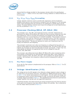
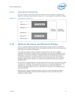
Test Access Port TAP Connection
 |
UPC - 735858204736
View all Intel BX80601920 manuals
Add to My Manuals
Save this manual to your list of manuals |
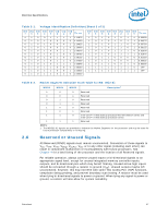
Page 19 highlights
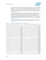
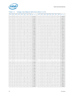
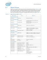
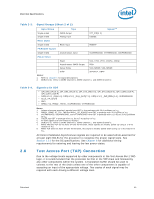
Electrical Specifications Table 2-3. Signal Groups (Sheet 2 of 2) Signal Group Type Signals1,2 Single ended Single ended CMOS Output Analog Input VTT_VID[4:2] ISENSE Reset Signal Single ended Reset Input RESET# PWRGOOD Signals Single ended Asynchronous Input VCCPWRGOOD, VTTPWRGOOD, VDDPWRGOOD Power/Other Power VCC, VTTA, VTTD, VCCPLL, VDDQ Asynchronous CMOS Output PSI# Sense Points VCC_SENSE, VSS_SENSE Other SKTOCC#, DBR# Notes: 1. Refer to Chapter 5 for signal descriptions. 2. DDR{0/1/2} refers to DDR3 Channel 0, DDR3 Channel 1, and DDR3 Channel 2. Table 2-4. Signals with ODT • QPI_DRX_DP[19:0], QPI_DRX_DN[19:0], QPI_DTX_DP[19:0], QPI_DTX_DN[19:0], QPI_CLKRX_D[N/P], QPI_CLKTX_D[N/P] • DDR{0/1/2}_DQ[63:0], DDR{0/1/2}_DQS_[N/P][7:0], DDR{0/1/2}_PAR_ERR#[0:2], VDDPWRGOOD • BCLK_ITP_D[N/P] • PECI • BPM#[7:0], PREQ#, TRST#, VCCPWRGOOD, VTTPWRGOOD Notes: 1. 2. Unless otherwise specified, signals have ODT in the PREQ#, BPM[7:0], TDI, TMS and BCLK_ITP_D[N/P] phaacvkeaOgeDTwiitnhp5a0ckagpeulwldiothwn35toVpSuSl.lup to VTT. 3. VCCPWRGOOD, VDDPWRGOOD, and VTTPWRGOOD have ODT in package with a 10 k to 20 k pulldown 4. TtoRSVTSS#. has ODT in package with a 1 k to 5 k pullup to VTT. 5. All DDR signals are terminated to VDDQ/2 6. DDR{0/1/2} refers to DDR3 Channel 0, DDR3 Channel 1, and DDR3 Channel 2. 7. While TMS and TDI do not have On-Die Termination, these signals are weakly pulled up using a 1-5 k resistor to VTT 8. While TCK does not have On-Die Termination, this signal is weakly pulled down using a 1-5 kresistor to VSS. All Control Sideband Asynchronous signals are required to be asserted/de-asserted for at least eight BCLKs for the processor to recognize the proper signal state. See Section 2.11 for the DC specifications. See Chapter 6 for additional timing requirements for entering and leaving the low power states. 2.8 Test Access Port (TAP) Connection Due to the voltage levels supported by other components in the Test Access Port (TAP) logic, it is recommended that the processor be first in the TAP chain and followed by any other components within the system. A translation buffer should be used to connect to the rest of the chain unless one of the other components is capable of accepting an input of the appropriate voltage. Two copies of each signal may be required with each driving a different voltage level. Datasheet 19
-
 1
1 -
2
-
3
-
4
-
5
-
6
-
7
-
8
-
9
-
10
-
11
-
12
-
13
-
 14
14 -
 15
15 -
 16
16 -
 17
17 -
 18
18 -
 19
19 -
 20
20 -
 21
21 -
 22
22 -
 23
23 -
 24
24 -
25
-
26
-
27
-
28
-
29
-
30
-
31
-
32
-
33
-
34
-
35
-
36
-
37
-
38
-
39
-
40
-
41
-
42
-
43
-
44
-
45
-
46
-
47
-
48
-
49
-
50
-
51
-
52
-
53
-
54
-
55
-
56
-
57
-
58
-
59
-
60
-
61
-
62
-
63
-
64
-
65
-
66
-
67
-
68
-
69
-
70
-
71
-
72
-
73
-
74
-
75
-
76
-
77
-
78
-
79
-
80
-
81
-
82
-
83
-
84
-
85
-
86
-
87
-
88
-
89
-
90
-
91
-
92
-
93
-
94
-
95
-
96
 |
 |
