Intel BX80601920 Data Sheet - Page 29
VCC_SENSE and VSS_SENSE lands.
 |
UPC - 735858204736
View all Intel BX80601920 manuals
Add to My Manuals
Save this manual to your list of manuals |
Page 29 highlights
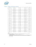
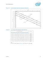
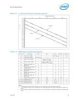
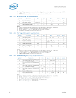
Electrical Specifications Table 2-15. Control Sideband Signal Group DC Specifications Symbol Parameter VIL Input Low Voltage VIH Input High Voltage VOL Output Low Voltage VOH Ron Ron ILI COMP0 Output High Voltage Buffer on Resistance Buffer on Resistance for VID[7:0] Input Leakage Current COMP Resistance Min - 0.76 * VTTA - VTTA 10 - - 49.4 Typ - - - - - 100 - 49.9 Max 0.64 * VTTA - VTT+A *RsRyOs_Nte/rm(R) ON - 18 - ± 200 50.40 Units V V V V A Notes: 1. Unless otherwise noted, all specifications in this table apply to all processor frequencies. 2. The VTTA referred to in these specifications refers to instantaneous VTTA. 3. For Vin between 0 V and VTTA. Measured when the driver is tristated. 4. VIH and VOH may experience excursions above VTT. 5. COMP resistance must be provided on the system board with 1% resistors. Notes1 2 2 2,4 2,4 3 5 2.11.2 VCC Overshoot Specification The processor can tolerate short transient overshoot events where VCC exceeds the VID voltage when transitioning from a high-to-low current load condition. This overshoot cannot exceed VID + VOS_MAX (VOS_MAX is the maximum allowable overshoot above VID). These specifications apply to the processor die voltage as measured across the VCC_SENSE and VSS_SENSE lands. Table 2-16. VCC Overshoot Specifications Symbol Parameter Min VOS_MAX Magnitude of VCCP overshoot above VID - TOS_MAX Time duration of VCCP overshoot above VID - Max 50 25 Units mV µs Figure 2-5 2-5 Notes Datasheet 29
-
 1
1 -
2
-
3
-
4
-
5
-
6
-
7
-
8
-
9
-
10
-
11
-
12
-
13
-
14
-
15
-
16
-
17
-
18
-
19
-
20
-
21
-
22
-
23
-
 24
24 -
 25
25 -
 26
26 -
 27
27 -
 28
28 -
 29
29 -
 30
30 -
 31
31 -
 32
32 -
 33
33 -
 34
34 -
35
-
36
-
37
-
38
-
39
-
40
-
41
-
42
-
43
-
44
-
45
-
46
-
47
-
48
-
49
-
50
-
51
-
52
-
53
-
54
-
55
-
56
-
57
-
58
-
59
-
60
-
61
-
62
-
63
-
64
-
65
-
66
-
67
-
68
-
69
-
70
-
71
-
72
-
73
-
74
-
75
-
76
-
77
-
78
-
79
-
80
-
81
-
82
-
83
-
84
-
85
-
86
-
87
-
88
-
89
-
90
-
91
-
92
-
93
-
94
-
95
-
96
 |
 |
