Intel BX80601920 Data Sheet - Page 68
Table 5-1., Signal Definitions Sheet 2 of 4
 |
UPC - 735858204736
View all Intel BX80601920 manuals
Add to My Manuals
Save this manual to your list of manuals |
Page 68 highlights
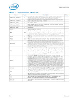
Signal Descriptions Table 5-1. Signal Definitions (Sheet 2 of 4) Name DDR{0/1/2}_MA[15:0] DDR{0/1/2}_ODT[3:0] DDR{0/1/2}_RAS# DDR{0/1/2}_RESET# DDR{0/1/2}_WE# ISENSE PECI PRDY# PREQ# PROCHOT# PSI# RESET# SKTOCC# TCK TDI TDO TESTLOW Type O O O O O I I/O O I/O I/O O I O I I O I Description Selects the Row address for Reads and writes, and the column address for activates. Also used to set values for DRAM configuration registers. Enables various combinations of termination resistance in the target and nontarget DIMMs when data is read or written Row Address Strobe. Resets DRAMs. Held low on power up, held high during self refresh, otherwise controlled by configuration register. Write Enable. Current sense from VRD11.1. PECI (Platform Environment Control Interface) is the serial sideband interface to the processor and is used primarily for thermal, power and error management. Details regarding the PECI electrical specifications, protocols and functions can be found in the Platform Environment Control Interface Specification. PRDY# is a processor output used by debug tools to determine processor debug readiness. PREQ# is used by debug tools to request debug operation of the processor. PROCHOT# will go active when the processor temperature monitoring sensor detects that the processor has reached its maximum safe operating temperature. This indicates that the processor Thermal Control Circuit has been activated, if enabled. This signal can also be driven to the processor to activate the Thermal Control Circuit. This signal does not have on-die termination and must be terminated on the system board. Processor Power Status Indicator signal. This signal is asserted when maximum possible processor core current consumption is less than 20A. Assertion of this signal is an indication that the VR controller does not currently need to be able to provide ICC above 20A, and the VR controller can use this information to move to more efficient operation point. This signal will de-assert at least 3.3 us before the current consumption will exceed 20A. The minimum PSI# assertion and de-assertion time is 1 BCLK. Asserting the RESET# signal resets the processor to a known state and invalidates its internal caches without writing back any of their contents. Note some PLL, QPI and error states are not effected by reset and only VCCPWRGOOD forces them to a known state. For a power-on Reset, RESET# must stay active for at least one millisecond after VCC and BCLK have reached their proper specifications. RESET# must not be kept asserted for more than 10 ms while VCCPWRGOOD is asserted. RESET# must be held de-asserted for at least 1 ms before it is asserted again. RESET# must be held asserted before VCCPWRGOOD is asserted. This signal does not have on-die termination and must be terminated on the system board. RESET# is a common clock signal. SKTOCC# (Socket Occupied) will be pulled to ground on the processor package. There is no connection to the processor silicon for this signal. System board designers may use this signal to determine if the processor is present. TCK (Test Clock) provides the clock input for the processor Test Bus (also known as the Test Access Port). TDI (Test Data In) transfers serial test data into the processor. TDI provides the serial input needed for JTAG specification support. TDO (Test Data Out) transfers serial test data out of the processor. TDO provides the serial output needed for JTAG specification support. TESTLOW must be connected to ground through a resistor for proper processor operation. Notes 68 Datasheet
-
 1
1 -
2
-
3
-
4
-
5
-
6
-
7
-
8
-
9
-
10
-
11
-
12
-
13
-
14
-
15
-
16
-
17
-
18
-
19
-
20
-
21
-
22
-
23
-
24
-
25
-
26
-
27
-
28
-
29
-
30
-
31
-
32
-
33
-
34
-
35
-
36
-
37
-
38
-
39
-
40
-
41
-
42
-
43
-
44
-
45
-
46
-
47
-
48
-
49
-
50
-
51
-
52
-
53
-
54
-
55
-
56
-
57
-
58
-
59
-
60
-
61
-
62
-
 63
63 -
 64
64 -
 65
65 -
 66
66 -
 67
67 -
 68
68 -
 69
69 -
 70
70 -
 71
71 -
 72
72 -
 73
73 -
74
-
75
-
76
-
77
-
78
-
79
-
80
-
81
-
82
-
83
-
84
-
85
-
86
-
87
-
88
-
89
-
90
-
91
-
92
-
93
-
94
-
95
-
96
 |
 |
