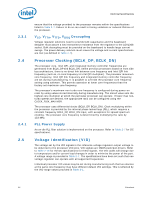
Intel BX80601920 Data Sheet - Page 15
Table 2-1., Voltage Identification Definition Sheet 1 of 3 - stepping
 |
UPC - 735858204736
View all Intel BX80601920 manuals
Add to My Manuals
Save this manual to your list of manuals |
Page 15 highlights
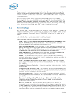
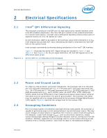
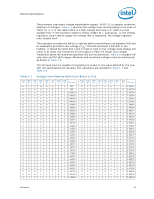
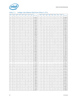
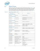
Electrical Specifications The processor uses eight voltage identification signals, VID[7:0], to support automatic selection of voltages. Table 2-1 specifies the voltage level corresponding to the state of VID[7:0]. A '1' in this table refers to a high voltage level and a '0' refers to a low voltage level. If the processor socket is empty (VID[7:0] = 11111111), or the voltage regulation circuit cannot supply the voltage that is requested, the voltage regulator must disable itself. The processor provides the ability to operate while transitioning to an adjacent VID and its associated processor core voltage (VCC). This will represent a DC shift in the loadline. It should be noted that a low-to-high or high-to-low voltage state change will result in as many VID transitions as necessary to reach the target core voltage. Transitions above the maximum specified VID are not permitted. Table 2-8 includes VID step sizes and DC shift ranges. Minimum and maximum voltages must be maintained as shown in Table 2-8. The VR used must be capable of regulating its output to the value defined by the new VID. DC specifications for dynamic VID transitions are included in Table 2-7 and Table 2-8 Table 2-1. Voltage Identification Definition (Sheet 1 of 3) VID 7 0 0 0 0 0 0 0 0 0 0 0 0 0 0 0 0 0 0 0 0 0 0 0 0 0 0 0 0 0 0 0 VID 6 0 0 0 0 0 0 0 0 0 0 0 0 0 0 0 0 0 0 0 0 0 0 0 0 0 0 0 0 0 0 0 VID 5 0 0 0 0 0 0 0 0 0 0 0 0 0 0 0 0 0 0 0 0 0 0 0 0 0 0 0 0 0 0 0 VID 4 0 0 0 0 0 0 0 0 0 0 0 0 0 0 0 0 1 1 1 1 1 1 1 1 1 1 1 1 1 1 1 VID 3 0 0 0 0 0 0 0 0 1 1 1 1 1 1 1 1 0 0 0 0 0 0 0 0 1 1 1 1 1 1 1 VID 2 0 0 0 0 1 1 1 1 0 0 0 0 1 1 1 1 0 0 0 0 1 1 1 1 0 0 0 0 1 1 1 VID 1 0 0 1 1 0 0 1 1 0 0 1 1 0 0 1 1 0 0 1 1 0 0 1 1 0 0 1 1 0 0 1 VID 0 VCC_MAX 0 OFF 1 OFF 0 1.60000 1 1.59375 0 1.58750 1 1.58125 0 1.57500 1 1.56875 0 1.56250 1 1.55625 0 1.55000 1 1.54375 0 1.53750 1 1.53125 0 1.52500 1 1.51875 0 1.51250 1 1.50625 0 1.50000 1 1.49375 0 1.48750 1 1.48125 0 1.47500 1 1.46875 0 1.46250 1 1.45625 0 1.45000 1 1.44375 0 1.43750 1 1.43125 0 1.42500 VID 7 0 0 0 0 0 0 0 0 0 0 0 0 0 0 0 0 0 0 0 0 0 0 0 0 0 0 0 0 0 0 0 VID 6 1 1 1 1 1 1 1 1 1 1 1 1 1 1 1 1 1 1 1 1 1 1 1 1 1 1 1 1 1 1 1 VID 5 0 0 0 0 0 1 1 1 1 1 1 1 1 1 1 1 1 1 1 1 1 1 1 1 1 1 1 1 1 1 1 VID VID 4 3 1 1 1 1 1 1 1 1 1 1 0 0 0 0 0 0 0 0 0 0 0 0 0 0 0 0 0 1 0 1 0 1 0 1 0 1 0 1 0 1 0 1 1 0 1 0 1 0 1 0 1 0 1 0 1 0 1 0 1 1 1 1 VID 2 0 1 1 1 1 0 0 0 0 1 1 1 1 0 0 0 0 1 1 1 1 0 0 0 0 1 1 1 1 0 0 VID 1 1 0 0 1 1 0 0 1 1 0 0 1 1 0 0 1 1 0 0 1 1 0 0 1 1 0 0 1 1 0 0 VID 0 1 0 1 0 1 0 1 0 1 0 1 0 1 0 1 0 1 0 1 0 1 0 1 0 1 0 1 0 1 0 1 VCC_MAX 1.04375 1.03750 1.03125 1.02500 1.01875 1.01250 1.00625 1.00000 0.99375 0.98750 0.98125 0.97500 0.96875 0.96250 0.95626 0.95000 0.94375 0.93750 0.93125 0.92500 0.91875 0.91250 0.90625 0.90000 0.89375 0.88750 0.88125 0.87500 0.86875 0.86250 0.85625 Datasheet 15
-
 1
1 -
2
-
3
-
4
-
5
-
6
-
7
-
8
-
9
-
 10
10 -
 11
11 -
 12
12 -
 13
13 -
 14
14 -
 15
15 -
 16
16 -
 17
17 -
 18
18 -
 19
19 -
 20
20 -
21
-
22
-
23
-
24
-
25
-
26
-
27
-
28
-
29
-
30
-
31
-
32
-
33
-
34
-
35
-
36
-
37
-
38
-
39
-
40
-
41
-
42
-
43
-
44
-
45
-
46
-
47
-
48
-
49
-
50
-
51
-
52
-
53
-
54
-
55
-
56
-
57
-
58
-
59
-
60
-
61
-
62
-
63
-
64
-
65
-
66
-
67
-
68
-
69
-
70
-
71
-
72
-
73
-
74
-
75
-
76
-
77
-
78
-
79
-
80
-
81
-
82
-
83
-
84
-
85
-
86
-
87
-
88
-
89
-
90
-
91
-
92
-
93
-
94
-
95
-
96
 |
 |
