Brother International IntelliFax-3550 Service Manual - Page 32
Main PCB, cuitry, and analog circuits for scanning, printing, and power transmission shifting.
 |
View all Brother International IntelliFax-3550 manuals
Add to My Manuals
Save this manual to your list of manuals |
Page 32 highlights
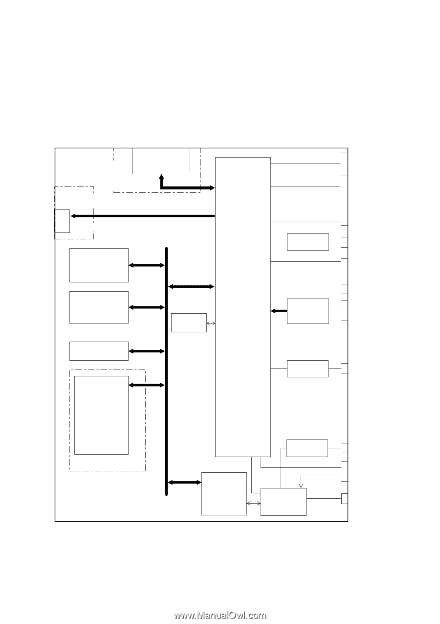
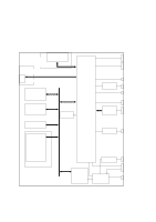
3.2 Main PCB The main PCB, which is the nucleus controlling the entire operation of the equipment, consists of a FAX engine (ASIC), memories, MODEM, motor drive circuits, sensor detection circuitry, and analog circuits for scanning, printing, and power transmission shifting. Centronics (MFC4450/ parallel interface 4550/4550plus/ 6550MC/7550MC/ 7650MC/9000/9500) Modular connector for PC interface (RS-232C) (FAX3550/3650/8000P/8200P) ROMs ASIC DRAM(s) E2PROM(s) Main PCB Control panel Relay PCB Main motor driver Image processor Fan 2 Main motor Solenoid Low-voltage power supply PCB Document sensor PCB Extended RAM connector Extended I/O connector for optional serial interface board (RS-232C and RS-422) (MFC6550MC/7550MC/ 7650MC/9000/9500) Scanner motor driver Scanner motor Amplifiers MODEM Analog switch operational amplifiers Speaker NCU PCB Hook switch PCB E2PROM: DRAM: Electrically Erasable Programmable Read-only Memory Dynamic Random Access Memory Block Diagram of Main PCB III - 13
-
 1
1 -
2
-
3
-
4
-
5
-
6
-
7
-
8
-
9
-
10
-
11
-
12
-
13
-
14
-
15
-
16
-
17
-
18
-
19
-
20
-
21
-
22
-
23
-
24
-
25
-
26
-
 27
27 -
 28
28 -
 29
29 -
 30
30 -
 31
31 -
 32
32 -
 33
33 -
 34
34 -
 35
35 -
 36
36 -
 37
37 -
38
-
39
-
40
-
41
-
42
-
43
-
44
-
45
-
46
-
47
-
48
-
49
-
50
-
51
-
52
-
53
-
54
-
55
-
56
-
57
-
58
-
59
-
60
-
61
-
62
-
63
-
64
-
65
-
66
-
67
-
68
-
69
-
70
-
71
-
72
-
73
-
74
-
75
-
76
-
77
-
78
-
79
-
80
-
81
-
82
-
83
-
84
-
85
-
86
-
87
-
88
-
89
-
90
-
91
-
92
-
93
-
94
-
95
-
96
-
97
-
98
-
99
-
100
-
101
-
102
-
103
-
104
-
105
-
106
-
107
-
108
-
109
-
110
-
111
-
112
-
113
-
114
-
115
-
116
-
117
-
118
-
119
-
120
-
121
-
122
-
123
-
124
-
125
-
126
-
127
-
128
-
129
-
130
-
131
-
132
-
133
-
134
-
135
-
136
-
137
-
138
-
139
-
140
-
141
-
142
-
143
-
144
-
145
-
146
-
147
-
148
-
149
-
150
-
151
-
152
-
153
-
154
-
155
-
156
-
157
-
158
-
159
-
160
-
161
-
162
-
163
-
164
-
165
-
166
-
167
-
168
-
169
-
170
-
171
-
172
-
173
-
174
-
175
-
176
-
177
-
178
-
179
-
180
-
181
-
182
-
183
-
184
-
185
-
186
-
187
-
188
-
189
-
190
-
191
 |
 |