Kyocera FS-1128MFP Service Manual - Page 244
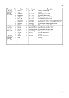
Scanner PWB silk-screen diagram, Connector, Signal, Voltage, Description, YC101
 |
View all Kyocera FS-1128MFP manuals
Add to My Manuals
Save this manual to your list of manuals |
Page 244 highlights
2JN 5 1 6 2 YC103 YC104 7 1 4 YC106 1 6 YC108 1 12 YC101 YC109 15 14 YC102 13 1 2 YC107 5 1 YC105 9 1 10 2 Figure 2-3-6Scanner PWB silk-screen diagram Connector Pin Signal YC101 1 +24V1 Connected 2 N.C. to the power 3 GND source PWB YC102 Connected to the control PWB YC103 Connected to the control PWB YC104 Connected to the ISU motor 1 SEGIR 2 SSDIR 3 SSBSY 4 SEGSI 5 SSCKN 6 SEGSO 7 PAGESET 8 OVMONOUT 9 CPURDY 10 CPUSEL 11 CPUSO 12 CPUSI 13 CPUCLK 14 +3.3V1 15 GND 1 +12V 2 GND 3 HPSW 4 GND 5 NC 6 LAMP 1 SCMOT1A 2 SCMOT2B 3 SCMOT1B 4 SCMOT2A I/O Voltage O 24 V DC -- -- Description 24 V DC power source Not used Ground O 0/3.3 V DC Serial communications interruption demand O 0/3.3 V DC Serial communications trans./recep. change O 0/3.3 V DC Impossible transmission/Completion notice I 0/3.3 V DC (pulse) Serial communications data output I 0/3.3 V DC (pulse) Serial communications clock O 0/3.3 V DC Vertical synchronizing signal I 0/3.3 V DC Vertical synchronizing monitor signal I 0/3.3 V DC Communications ready signal I 0/3.3 V DC Communications ready signal O 0/3.3 V DC Communications select signal I 0/3.3 V DC (pulse) Serial communications data input O 0/3.3 V DC (pulse) Serial communications data output O 0/3.3 V DC (pulse) Serial communications clock signal I 3.3 V DC 3.3 V DC power source -- Ground I 12 V DC 12 V DC power source -- Ground I 0/3.3 V DC Home position sensor: On/Off -- Ground -- Not used I 0/24 V DC Exposure lamp drive signal O 0/24 V DC (pulse) ISU motor drive pulse O 0/24 V DC (pulse) ISU motor drive pulse O 0/24 V DC (pulse) ISU motor drive pulse O 0/24 V DC (pulse) ISU motor drive pulse 2-3-10
-
 1
1 -
2
-
3
-
4
-
5
-
6
-
7
-
8
-
9
-
10
-
11
-
12
-
13
-
14
-
15
-
16
-
17
-
18
-
19
-
20
-
21
-
22
-
23
-
24
-
25
-
26
-
27
-
28
-
29
-
30
-
31
-
32
-
33
-
34
-
35
-
36
-
37
-
38
-
39
-
40
-
41
-
42
-
43
-
44
-
45
-
46
-
47
-
48
-
49
-
50
-
51
-
52
-
53
-
54
-
55
-
56
-
57
-
58
-
59
-
60
-
61
-
62
-
63
-
64
-
65
-
66
-
67
-
68
-
69
-
70
-
71
-
72
-
73
-
74
-
75
-
76
-
77
-
78
-
79
-
80
-
81
-
82
-
83
-
84
-
85
-
86
-
87
-
88
-
89
-
90
-
91
-
92
-
93
-
94
-
95
-
96
-
97
-
98
-
99
-
100
-
101
-
102
-
103
-
104
-
105
-
106
-
107
-
108
-
109
-
110
-
111
-
112
-
113
-
114
-
115
-
116
-
117
-
118
-
119
-
120
-
121
-
122
-
123
-
124
-
125
-
126
-
127
-
128
-
129
-
130
-
131
-
132
-
133
-
134
-
135
-
136
-
137
-
138
-
139
-
140
-
141
-
142
-
143
-
144
-
145
-
146
-
147
-
148
-
149
-
150
-
151
-
152
-
153
-
154
-
155
-
156
-
157
-
158
-
159
-
160
-
161
-
162
-
163
-
164
-
165
-
166
-
167
-
168
-
169
-
170
-
171
-
172
-
173
-
174
-
175
-
176
-
177
-
178
-
179
-
180
-
181
-
182
-
183
-
184
-
185
-
186
-
187
-
188
-
189
-
190
-
191
-
192
-
193
-
194
-
195
-
196
-
197
-
198
-
199
-
200
-
201
-
202
-
203
-
204
-
205
-
206
-
207
-
208
-
209
-
210
-
211
-
212
-
213
-
214
-
215
-
216
-
217
-
218
-
219
-
220
-
221
-
222
-
223
-
224
-
225
-
226
-
227
-
228
-
229
-
230
-
231
-
232
-
233
-
234
-
235
-
236
-
237
-
238
-
 239
239 -
 240
240 -
 241
241 -
 242
242 -
 243
243 -
 244
244 -
 245
245 -
 246
246 -
 247
247 -
 248
248 -
 249
249 -
250
-
251
-
252
 |
 |
