HP Integrity rx2620 Installation Guide, Third Edition - HP Integrity rx2620 (A - Page 21
Processor Sockets, Processor Bus, ZX1 I/O and Memory Controller, System Memory
 |
View all HP Integrity rx2620 manuals
Add to My Manuals
Save this manual to your list of manuals |
Page 21 highlights
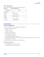
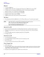
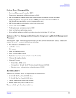
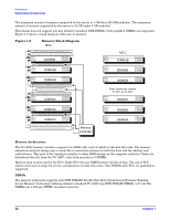
Introduction System Board Components • "Dual Serial Controller" on page 24 • "Field Programmable Gate Array" on page 24 • "Baseboard Management Controller" on page 24 • "SCSI Controller" on page 25 • "IDE Interface" on page 25 • "1 Gb System LAN" on page 25 • "USB Connectors" on page 25 • "User Interface" on page 26 • "Event IDs for Errors and Events" on page 26 Processor Sockets The system board consists of two zero insertion force (ZIF) processor sockets, the core electronic complex (CEC), and circuitry for clock and power generation and distribution, boundary scan, in-target probe, and debug. The front side bus (FSB) is the IA64 processor bus, based on bus protocol from Intel. Unlike previous PA-RISC microprocessors that utilized HP's proprietary processor bus, this processor is designed to utilize the FSB. This allows processor field replaceable units (FRUs) to be dropped in, provided that electrical and mechanical compatibility and support circuitry exist. For the purposes of this document, a FRU consists of a single processor with power pod, and the heatsink assembly. Each processor plugs directly into, and is powered by its own 12 V to 1.2 V power pod. Other power for the system board comes from multiple on-board DC to DC converters. Each processor is attached to the board through a ZIF socket and the entire FRU secured by a heatsink. Processor Bus The FSB runs at 200 MHz. Data on the FSB are transferred at a double data rate, which allows a peak FSB bandwidth of 6.4 Gb/sec. ZX1 I/O and Memory Controller The HP Integrity rx2620 server supports the following features of the ZX1 I/O and memory controller chip: • 8.5 Gb/s peak I/O bandwidth • Seven communication paths • Peak memory bandwidth of 8.5 Gb/s. • Two memory cells, 144 data bits each. System Memory The memory subsystem provides two memory cells, each of which is 144 data bits wide. Each cell has six DIMM slots, which means a total of 12 DIMM slots are available. The memory bus clock speed is 133 MHz, and the data transfer rate is 266 Mtransfers/second as data is clocked on both edges of the clock. The peak data bandwidth for this memory subsystem design is 8.5 Gb/s. Load DIMMs in quads with qualified modules. Memory is protected by data ECC, and the hardware implementation supports chip-spare. Chapter 1 21
-
 1
1 -
2
-
3
-
4
-
5
-
6
-
7
-
8
-
9
-
10
-
11
-
12
-
13
-
14
-
15
-
 16
16 -
 17
17 -
 18
18 -
 19
19 -
 20
20 -
 21
21 -
 22
22 -
 23
23 -
 24
24 -
 25
25 -
 26
26 -
27
-
28
-
29
-
30
-
31
-
32
-
33
-
34
-
35
-
36
-
37
-
38
-
39
-
40
-
41
-
42
-
43
-
44
-
45
-
46
-
47
-
48
-
49
-
50
-
51
-
52
-
53
-
54
-
55
-
56
-
57
-
58
-
59
-
60
-
61
-
62
-
63
-
64
-
65
-
66
-
67
-
68
-
69
-
70
-
71
-
72
-
73
-
74
-
75
-
76
-
77
-
78
-
79
-
80
-
81
-
82
-
83
-
84
-
85
-
86
-
87
-
88
-
89
-
90
-
91
-
92
-
93
-
94
-
95
-
96
-
97
-
98
-
99
-
100
-
101
-
102
-
103
-
104
-
105
-
106
-
107
-
108
-
109
 |
 |