Intel X38ML Product Specification - Page 21
Memory Controller Hub MCH: Intel, I/O Controller Hub: Intel - drivers
 |
UPC - 735858197397
View all Intel X38ML manuals
Add to My Manuals
Save this manual to your list of manuals |
Page 21 highlights
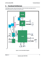
Intel® Server Board X38ML Functional Architecture The following sub-sections provide an overview of the primary functions and supported features of each chipset component as they are used on the Intel® Server Board X38ML. Later sections provide more detail on the implementation of the subsystems. 3.2.1 Memory Controller Hub (MCH): Intel® X38 MCH The MCH integrates four interfaces: 1. Processor/host interface (FSB) - Supports LGA775 processors in a UP System configuration - 200/266/333 MHz FSB clock frequency. Supports FSB transfer rates of 800/1066/1333 MT/s. - GTL+ bus drivers with integrated GTL termination resistors 2. System memory interface (memory controller) - Supports 512 Mbit, and 1 Gbit memory technologies - DDR2 - 667, 800 MHz - 8 GB addressable memory - Supports unbuffered, ECC, and non-ECC DIMM 3. Direct media interface (DMI) interface - Interface to the Intel® ICH9R South Bridge - 100 MHz reference clock shared with PCI Express* interface(s) 4. PCI Express* interface - Contains two PCI Express* x16 ports. One PCI Express* x16 port is connected to one PCI Express* X16 connector as shown in the block diagram. - Compliant with the PCI Express* base specification revision 2.0. 3.2.2 I/O Controller Hub: Intel® ICH9-R The Intel® ICH9-R component integrates bridge functionality for PCI Express*, LPC, USB, SATA II, IDE and SMBus, and numerous board management functions. The ICH9R is packaged in a 31 mm x 31 mm 676 pin mBGA. 3.2.2.1 Direct Media Interface (DMI) DMI is the name given to chip-to-chip connection between the Intel® X38 MCH and the Intel® ICH9-R. DMI is an X4 link that mostly adheres to the PCI Express* specification. Deviations of the DMI from standard PCI Express* specifications are described in the Intel® ICH9 component specification. 3.2.2.2 PCI Express* Interfaces The Intel® ICH9R provides six PCI Express* Root Ports (GEN1), which are compliant with the PCI Express Base Specification, Revision 1.1. The PCI Express* root ports 1-4 can be statically configured as four x 1 ports, or ganged together to form two x 2 ports, one x 2 with two x1 ports, or one x4 port. Ports 5 and 6 can be used as two x1 ports or one x2. The x4 configuration supports lane reversal. Each Root Port fully supports 2.5 Gb/s bandwidth in each direction. Revision 1.3 9 Intel order number E15331-006
-
 1
1 -
2
-
3
-
4
-
5
-
6
-
7
-
8
-
9
-
10
-
11
-
12
-
13
-
14
-
15
-
 16
16 -
 17
17 -
 18
18 -
 19
19 -
 20
20 -
 21
21 -
 22
22 -
 23
23 -
 24
24 -
 25
25 -
 26
26 -
27
-
28
-
29
-
30
-
31
-
32
-
33
-
34
-
35
-
36
-
37
-
38
-
39
-
40
-
41
-
42
-
43
-
44
-
45
-
46
-
47
-
48
-
49
-
50
-
51
-
52
-
53
-
54
-
55
-
56
-
57
-
58
-
59
-
60
-
61
-
62
-
63
-
64
-
65
-
66
-
67
-
68
-
69
-
70
-
71
-
72
-
73
-
74
-
75
-
76
-
77
-
78
-
79
-
80
-
81
-
82
-
83
-
84
-
85
-
86
-
87
-
88
-
89
-
90
-
91
-
92
-
93
-
94
-
95
-
96
-
97
-
98
-
99
-
100
-
101
-
102
-
103
-
104
-
105
-
106
-
107
-
108
-
109
-
110
-
111
-
112
-
113
-
114
-
115
-
116
-
117
-
118
-
119
-
120
-
121
-
122
-
123
-
124
-
125
-
126
-
127
-
128
-
129
-
130
-
131
-
132
 |
 |