Nintendo 1504166 Programming Manual - Page 15
System Configuration, 2.1 CPU Block Diagram
 |
View all Nintendo 1504166 manuals
Add to My Manuals
Save this manual to your list of manuals |
Page 15 highlights
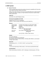
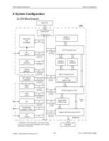
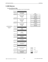
AGB Programming Manual 2 System Configuration 2.1 CPU Block Diagram Game Pak 16 ARM7TDMI CPU (16.78MHz) Game Pak I/F (Prefetch Buffer) 32 System Configuration CPU VRAM_A (64KByte) 16 INT Control ROM (16KByte) 32 R:8/16/32 W:8/16/32 32 R:8/16/32 16 R:16/32 W:16/32 BG Processing Circuit 16 16 VRAM_B (16KByte) VRAM_C (16KByte) 16 16 16 16 16 16 16 WRAM (32KByte) EXT. WRAM (256KByte) DMAC (4ch) Timer (4ch) SIO SOUND(CGB compatible + PWM) 32 R:8/16/32 W:8/16/32 16(2 Wait) R:8/16/32 W:8/16/32 32 R:8/16/32 W:8/16/32 32 R:8/16/32 W:8/16/32 32 R:8/16/32 W:8/16/32 32 KEY Control 32 32 32 R:16/32 W:16/32 OBJ Processing Circuit OAM (64bit x 128) 32 R:16/32 W:16/32 Priority Evaluation Circuit 16 R:16/32 W:16/32 Palette RAM (16bit x 512) Bitmap Mode 32 R:8/16/32 W:8/16/32 Special Color Processing Circuit RGB(5:5:5) 16 * "R:8/16/32" and "W:8/16/32" mean that you can access an area of 8bits/16bits/32bits when reading and writing, respectively. LCD Unit ©1999 - 2001 Nintendo of America Inc. 15 D.C.N. AGB-06-0001-002B4
-
 1
1 -
2
-
3
-
4
-
5
-
6
-
7
-
8
-
9
-
 10
10 -
 11
11 -
 12
12 -
 13
13 -
 14
14 -
 15
15 -
 16
16 -
 17
17 -
 18
18 -
 19
19 -
 20
20 -
21
-
22
-
23
-
24
-
25
-
26
-
27
-
28
-
29
-
30
-
31
-
32
-
33
-
34
-
35
-
36
-
37
-
38
-
39
-
40
-
41
-
42
-
43
-
44
-
45
-
46
-
47
-
48
-
49
-
50
-
51
-
52
-
53
-
54
-
55
-
56
-
57
-
58
-
59
-
60
-
61
-
62
-
63
-
64
-
65
-
66
-
67
-
68
-
69
-
70
-
71
-
72
-
73
-
74
-
75
-
76
-
77
-
78
-
79
-
80
-
81
-
82
-
83
-
84
-
85
-
86
-
87
-
88
-
89
-
90
-
91
-
92
-
93
-
94
-
95
-
96
-
97
-
98
-
99
-
100
-
101
-
102
-
103
-
104
-
105
-
106
-
107
-
108
-
109
-
110
-
111
-
112
-
113
-
114
-
115
-
116
-
117
-
118
-
119
-
120
-
121
-
122
-
123
-
124
-
125
-
126
-
127
-
128
-
129
-
130
-
131
-
132
-
133
-
134
-
135
-
136
-
137
-
138
-
139
-
140
-
141
-
142
-
143
-
144
-
145
-
146
-
147
-
148
-
149
-
150
-
151
-
152
-
153
-
154
-
155
-
156
-
157
-
158
-
159
-
160
-
161
-
162
-
163
-
164
-
165
-
166
-
167
-
168
-
169
-
170
-
171
 |
 |
