Nintendo 1504166 Programming Manual - Page 16
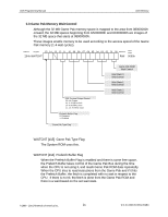
Complete Block Diagram, AGB Programming Manual, System Configuration
 |
View all Nintendo 1504166 manuals
Add to My Manuals
Save this manual to your list of manuals |
Page 16 highlights
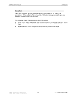
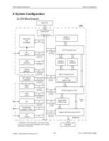
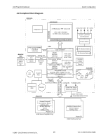
AGB Programming Manual System Configuration 2.2 Complete Block Diagram AGB Unit LCD Module External Unit Infrared Communi -cation Adaptor, etc. LCD Driver RGB Regulator IC 2.9"Reflective TFT Color LCD 240 x 160 x RGB Dot 32,768 Colors Displayable LCD Driver LCD Driver LCD Driver -15V 2.5V 3.3V 5V 13.6V DC-DC Converter and Regulator Power Switch CPU External WRAM 256KByte 16bit Bus 2wait 6Pin-EXP SIO Communication 8/32bit SIO General Purpose Port Multi-SIO UART JOY CPU LCD Controller VRAM 98KByte 16bit Bus CPU Internal WRAM 32KByte 32bit Bus AGB System ROM 16KByte 32bit Bus AGB 32bit CPU Core ARM7TDMI CGB 8bit CPU Core CGB System ROM 2KB Sound Volume Sound Amp Peripheral Circuit (SOUND, DMA, TIMER, I/O, etc) Prefetch Buffer 16bit x 8 AA Alkaline Battery AA Alkaline Battery 3.3V/5V Voltage Detection Circuit L Controller R A B SELECT START 4.194MHz (System 16.78MHz) 3.3V(AGB) 5V(DMG/CGB) Headphone Jack Speaker Game Pak Shape Detection Switch Switch Between AD Bus/ General Purpose Bus Gane Pak Game Pak Power 3.3V(AGB)/5V(DMG/CGB) General Purpose Bus Memory Space 64KByte Max. AD Bus Memory Space 32MByte Max. Power 3.3V AGB Game Pak(AGB Only) General Purpose Bus Memory Space 32KByte Max. Power 5V DMG/CGB Game Pak ©1999 - 2001 Nintendo of America Inc. 16 D.C.N. AGB-06-0001-002B4
-
 1
1 -
2
-
3
-
4
-
5
-
6
-
7
-
8
-
9
-
10
-
 11
11 -
 12
12 -
 13
13 -
 14
14 -
 15
15 -
 16
16 -
 17
17 -
 18
18 -
 19
19 -
 20
20 -
 21
21 -
22
-
23
-
24
-
25
-
26
-
27
-
28
-
29
-
30
-
31
-
32
-
33
-
34
-
35
-
36
-
37
-
38
-
39
-
40
-
41
-
42
-
43
-
44
-
45
-
46
-
47
-
48
-
49
-
50
-
51
-
52
-
53
-
54
-
55
-
56
-
57
-
58
-
59
-
60
-
61
-
62
-
63
-
64
-
65
-
66
-
67
-
68
-
69
-
70
-
71
-
72
-
73
-
74
-
75
-
76
-
77
-
78
-
79
-
80
-
81
-
82
-
83
-
84
-
85
-
86
-
87
-
88
-
89
-
90
-
91
-
92
-
93
-
94
-
95
-
96
-
97
-
98
-
99
-
100
-
101
-
102
-
103
-
104
-
105
-
106
-
107
-
108
-
109
-
110
-
111
-
112
-
113
-
114
-
115
-
116
-
117
-
118
-
119
-
120
-
121
-
122
-
123
-
124
-
125
-
126
-
127
-
128
-
129
-
130
-
131
-
132
-
133
-
134
-
135
-
136
-
137
-
138
-
139
-
140
-
141
-
142
-
143
-
144
-
145
-
146
-
147
-
148
-
149
-
150
-
151
-
152
-
153
-
154
-
155
-
156
-
157
-
158
-
159
-
160
-
161
-
162
-
163
-
164
-
165
-
166
-
167
-
168
-
169
-
170
-
171
 |
 |
