Epson 680Pro Service Manual - Page 43
C383 MAIN Board, Block Diagram for the C383 MAIN Board
 |
UPC - 010343832138
View all Epson 680Pro manuals
Add to My Manuals
Save this manual to your list of manuals |
Page 43 highlights
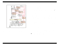
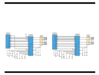
EPSON Stylus COLOR 680/777/77i 2.2.2 C383 MAIN Board The printer mechanism is controlled by C383 MAIN. See Figure for the C383 MAIN board block diagram. Revision B o Use of the 3.3V chips in the logic circuit The 3.3 V regulator (IC11) on the C383MAIN produces 3.3 V by pressuring down the 5.5 VDC, also generated on this board, to drive several chips. See the table below that separately shows the chips driven by the +5V and +3V. Table 2-6. 3.3V Drive Chips & 5.5V Drive Chips +5V 3.3V Sensors I/F Circuit PNL Board CPU P-ROM D-RAM o Timer IC & Lithium battery are not mounted Unlike the previous products, the Timer IC and the Lithium battery are not mounted on the Main board. So, this product perform the Power-on cleaning or Timer cleaning based on the time command which is sent from the printer driver. o D-RAM 4Mbit and 16Mbit D-RAMS are mounted on the Main board. o One CPU controls the all function on the main board. Figure 2-17. Block Diagram for the C383 MAIN Board Following shows you the major characteristic of this main board. Operating Principles Electrical Circuit Operating Principles 43
-
 1
1 -
2
-
3
-
4
-
5
-
6
-
7
-
8
-
9
-
10
-
11
-
12
-
13
-
14
-
15
-
16
-
17
-
18
-
19
-
20
-
21
-
22
-
23
-
24
-
25
-
26
-
27
-
28
-
29
-
30
-
31
-
32
-
33
-
34
-
35
-
36
-
37
-
 38
38 -
 39
39 -
 40
40 -
 41
41 -
 42
42 -
 43
43 -
 44
44 -
 45
45 -
 46
46 -
 47
47 -
 48
48 -
49
-
50
-
51
-
52
-
53
-
54
-
55
-
56
-
57
-
58
-
59
-
60
-
61
-
62
-
63
-
64
-
65
-
66
-
67
-
68
-
69
-
70
-
71
-
72
-
73
-
74
-
75
-
76
-
77
-
78
-
79
-
80
-
81
-
82
-
83
-
84
-
85
-
86
-
87
-
88
-
89
-
90
-
91
-
92
-
93
-
94
-
95
-
96
-
97
-
98
-
99
-
100
-
101
-
102
-
103
-
104
-
105
-
106
-
107
-
108
-
109
-
110
-
111
-
112
-
113
-
114
-
115
-
116
-
117
-
118
-
119
-
120
-
121
-
122
-
123
-
124
-
125
-
126
-
127
-
128
-
129
-
130
-
131
-
132
-
133
-
134
-
135
-
136
-
137
-
138
-
139
-
140
-
141
-
142
-
143
-
144
-
145
 |
 |
