Intel BX80605I7870 Data Sheet
Intel BX80605I7870 - Core i7 2.93 GHz Processor Manual
 |
UPC - 735858210461
View all Intel BX80605I7870 manuals
Add to My Manuals
Save this manual to your list of manuals |
Intel BX80605I7870 manual content summary:
- Intel BX80605I7870 | Data Sheet - Page 1
Intel® Core™ i7 Processor Extreme Edition and Intel® Core™ i7 Processor Datasheet, Volume 2 November 2008 Document Number: 320835-002 - Intel BX80605I7870 | Data Sheet - Page 2
features or instructions marked "reserved" or "undefined." Intel reserves these for future definition and shall have no responsibility whatsoever for conflicts or incompatibilities arising from future changes to them. The Intel® Core™ i7 Processor Extreme Edition and Intel® Core™ i7 Processor may - Intel BX80605I7870 | Data Sheet - Page 3
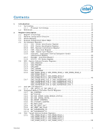
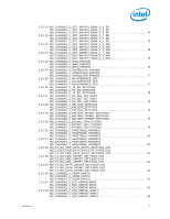
Contents 1 Introduction ...11 1.1 Terminology ...11 1.1.1 Processor Terminology 11 1.2 References ...13 2 Register Description 15 2.1 Register Terminology 15 2.2 Platform Configuration SAD_INTERLEAVE_LIST_6, SAD_INTERLEAVE_LIST_7 47 2.7 Intel QPI Link Registers 48 2.7.1 - Intel BX80605I7870 | Data Sheet - Page 4
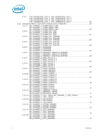
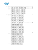
2.10 2.9.2 TAD_INTERLEAVE_LIST_0, TAD_INTERLEAVE_LIST_1 TAD_INTERLEAVE_LIST_2, TAD_INTERLEAVE_LIST_3 TAD_INTERLEAVE_LIST_4, TAD_INTERLEAVE_LIST_5 TAD_INTERLEAVE_LIST_6, TAD_INTERLEAVE_LIST_7 59 Integrated Memory Controller Channel Control Registers 60 2.10.1 MC_CHANNEL_0_DIMM_RESET_CMD - Intel BX80605I7870 | Data Sheet - Page 5
2.10.19 MC_CHANNEL_0_ODT_MATRIX_RANK_0_3_RD MC_CHANNEL_1_ODT_MATRIX_RANK_0_3_RD MC_CHANNEL_2_ODT_MATRIX_RANK_0_3_RD 74 2.10.20 MC_CHANNEL_0_ODT_MATRIX_RANK_4_7_RD MC_CHANNEL_1_ODT_MATRIX_RANK_4_7_RD MC_CHANNEL_2_ODT_MATRIX_RANK_4_7_RD 75 2.10.21 MC_CHANNEL_0_ODT_MATRIX_RANK_0_3_WR - Intel BX80605I7870 | Data Sheet - Page 6
2.11 2.12 2.10.39 Error Injection Implementation 84 Integrated Memory Controller Channel Address Registers 85 2.11.1 MC_DOD_CH0_0, MC_DOD_CH0_1, MC_DOD_CH0_2 85 2.11.2 MC_DOD_CH1_0, MC_DOD_CH1_1, MC_DOD_CH1_2 86 2.11.3 MC_DOD_CH2_0, MC_DOD_CH2_1, MC_DOD_CH2_2 87 2.11.4 MC_SAG_CH0_0, - Intel BX80605I7870 | Data Sheet - Page 7
2.13 2.14 MC_RIR_WAY_CH2_6, MC_RIR_WAY_CH2_7 MC_RIR_WAY_CH2_8, MC_RIR_WAY_CH2_9 MC_RIR_WAY_CH2_10, MC_RIR_WAY_CH2_11 MC_RIR_WAY_CH2_12, MC_RIR_WAY_CH2_13 MC_RIR_WAY_CH2_14, MC_RIR_WAY_CH2_15 MC_RIR_WAY_CH2_16, MC_RIR_WAY_CH2_17 MC_RIR_WAY_CH2_18, MC_RIR_WAY_CH2_19 MC_RIR_WAY_CH2_20, - Intel BX80605I7870 | Data Sheet - Page 8
Functions Specifically Handled by the Processor 18 2-2 Device 0, Function 0: Generic Non-core Registers 19 2-3 Device 0, Function 1: System Address Decoder Registers 20 2-4 Device 2, Function 0: Intel QPI Link 0 Registers 21 2-5 Device 2, Function 1: Intel QPI Physical 0 Registers 22 2-6 Device - Intel BX80605I7870 | Data Sheet - Page 9
Revision History Revision Number -001 -002 Initial release. Updated section 2.2 and Table 2.3. Description Date November 2008 November 2008 Datasheet 9 - Intel BX80605I7870 | Data Sheet - Page 10
10 Datasheet - Intel BX80605I7870 | Data Sheet - Page 11
™ i7 processor are multi-core processors, based on 45 nm process technology. Processor features vary by component and include up to two Intel QuickPath Interconnect point to point links capable of up to 6.4 GT/s, up to 8 MB of shared cache, and an integrated memory controller. The processors support - Intel BX80605I7870 | Data Sheet - Page 12
free air. Under these conditions, processor lands should not be connected to any supply voltages, have any I/Os biased, or receive any clocks. • Intel® Core™ i7 processor Extreme Edition and Intel® Core™ i7 processor - The desktop product, including processor substrate and integrated heat spreader - Intel BX80605I7870 | Data Sheet - Page 13
Intel® Core™ i7 Processor Datasheet, Volume 1 Intel® Core™ i7 Processor Extreme Edition and Intel® Core™ i7 Processor and LGA1366 Socket Thermal and Mechanical Design Guide Intel® 64 and IA-32 Intel® Architecture Software Developer's Manual • Volume 1: Basic Architecture • Volume 2A: Instruction - Intel BX80605I7870 | Data Sheet - Page 14
Introduction 14 Datasheet - Intel BX80605I7870 | Data Sheet - Page 15
. This document highlights registers which do not apply to all processor components. Refer to the particular processor's Specification Update for a list of features supported. Register Terminology Registers and register bits are assigned one or more of the following attributes. These attributes - Intel BX80605I7870 | Data Sheet - Page 16
processor non-core. Device 0, Function 0 contains the generic non-core configuration registers for the processor and resides at DID (Device ID) of 2C41h. Device 0, Function 1 contains the System Address Decode registers and resides at DID of 2C01h. • Device 2: Intel to processors supporting - Intel BX80605I7870 | Data Sheet - Page 17
Processor Component Register Group Intel QuickPath Architecture Generic Non-core Registers Intel QuickPath Architecture System Address Decoder Intel QPI Link 0 Intel 1 5 2 3 0 1 6 2 3 Notes: 1. Applies only to processors supporting sparing, mirroring, and scrubbing RAS features. Datasheet 17 - Intel BX80605I7870 | Data Sheet - Page 18
2.4 Detailed Configuration Space Maps Table 2-2. Device 0, Function 0: Generic Non-core Registers DID PCISTS CCR HDR SID VID 00h PCICMD 04h RID 08h 0Ch 10h 14h 18h 1Ch 20h 24h 28h SVID 2Ch 30h 34h 38h - Intel BX80605I7870 | Data Sheet - Page 19
Register Description Table 2-3. Device 0, Function 1: System Address Decoder Registers DID VID 00h PCISTS PCICMD 04h CCR RID 08h HDR 0Ch 10h 14h 18h 1Ch 20h 24h 28h SID SVID 2Ch 30h 34h 38h 3Ch SAD_PAM0123 40h SAD_PAM456 44h SAD_HEN 48h SAD_SMRAM 4Ch SAD_PCIEXBAR - Intel BX80605I7870 | Data Sheet - Page 20
Table 2-4. Device 2, Function 0: Intel QPI Link 0 Registers DID PCISTS VID 00h PCICMD 04h CCR RID 08h HDR 0Ch 10h 14h 18h 1Ch 20h 24h 28h SID SVID 2Ch 30h - Intel BX80605I7870 | Data Sheet - Page 21
Register Description Table 2-5. Device 2, Function 1: Intel QPI Physical 0 Registers DID PCISTS VID 00h PCICMD 04h CCR RID 08h HDR SID 0Ch 10h 14h 18h 1Ch 20h 24h 28h SVID 2Ch 30h - Intel BX80605I7870 | Data Sheet - Page 22
Register Description Table 2-6. Device 3, Function 0: Integrated Memory Controller Registers DID VID 00h PCISTS PCICMD 04h CCR RID 08h HDR 0Ch 10h 14h 18h 1Ch 20h 24h 28h SID SVID 2Ch 30h 34h 38h 3Ch 40h 44h MC_CONTROL 48h MC_STATUS 4Ch MC_SMI_SPARE_DIMM_ERROR_STATUS - Intel BX80605I7870 | Data Sheet - Page 23
Register Description Table 2-7. Device 3, Function 1: Target Address Decoder Registers DID PCISTS CCR HDR SID VID 00h PCICMD 04h RID 08h 0Ch 10h 14h 18h 1Ch 20h 24h 28h SVID 2Ch 30h 34h 38h 3Ch 40h 44h 48h 4Ch 50h 54h 58h 5Ch 60h 64h 68h 6Ch 70h 74h 78h 7Ch - Intel BX80605I7870 | Data Sheet - Page 24
Register Description Table 2-8. Device 4, Function 0: Integrated Memory Controller Channel 0 Control Registers DID PCISTS CCR HDR VID PCICMD RID SID SVID MC_CHANNEL_0_DIMM_RESET_CMD MC_CHANNEL_0_DIMM_INIT_CMD MC_CHANNEL_0_DIMM_INIT_PARAMS MC_CHANNEL_0_DIMM_INIT_STATUS MC_CHANNEL_0_DDR3CMD - Intel BX80605I7870 | Data Sheet - Page 25
Register Description Table 2-9. Device 4, Function 1: Integrated Memory Controller Channel 0 Address Registers DID VID 00h PCISTS PCICMD 04h CCR RID 08h HDR 0Ch 10h 14h 18h 1Ch 20h 24h 28h SID SVID 2Ch 30h 34h 38h 3Ch 40h 44h MC_DOD_CH0_0 48h MC_DOD_CH0_1 4Ch - Intel BX80605I7870 | Data Sheet - Page 26
Register Description Table 2-10. Device 4, Function 2: Integrated Memory Controller Channel 0 Rank Registers DID PCISTS CCR HDR VID PCICMD RID SID SVID MC_RIR_LIMIT_CH0_0 MC_RIR_LIMIT_CH0_1 MC_RIR_LIMIT_CH0_2 MC_RIR_LIMIT_CH0_3 MC_RIR_LIMIT_CH0_4 MC_RIR_LIMIT_CH0_5 MC_RIR_LIMIT_CH0_6 - Intel BX80605I7870 | Data Sheet - Page 27
Register Description Table 2-11. Device 4, Function 3: Integrated Memory Controller Channel 0 Thermal Control Registers DID VID 00h PCISTS PCICMD 04h CCR RID 08h HDR 0Ch 10h 14h 18h 1Ch 20h 24h 28h SID SVID 2Ch 30h 34h 38h 3Ch 40h 44h MC_THERMAL_CONTROL0 48h - Intel BX80605I7870 | Data Sheet - Page 28
Register Description Table 2-12. Device 5, Function 0: Integrated Memory Controller Channel 1 Control Registers DID PCISTS CCR HDR VID PCICMD RID SID SVID MC_CHANNEL_1_DIMM_RESET_CMD MC_CHANNEL_1_DIMM_INIT_CMD MC_CHANNEL_1_DIMM_INIT_PARAMS MC_CHANNEL_1_DIMM_INIT_STATUS MC_CHANNEL_1_DDR3CMD - Intel BX80605I7870 | Data Sheet - Page 29
Register Description Table 2-13. Device 5, Function 1: Integrated Memory Controller Channel 1 Address Registers DID VID 00h PCISTS PCICMD 04h CCR RID 08h HDR 0Ch 10h 14h 18h 1Ch 20h 24h 28h SID SVID 2Ch 30h 34h 38h 3Ch 40h 44h MC_DOD_CH1_0 48h MC_DOD_CH1_1 4Ch - Intel BX80605I7870 | Data Sheet - Page 30
Register Description Table 2-14. Device 5, Function 2: Integrated Memory Controller Channel 1 Rank Registers DID PCISTS CCR HDR VID PCICMD RID SID SVID MC_RIR_LIMIT_CH1_0 MC_RIR_LIMIT_CH1_1 MC_RIR_LIMIT_CH1_2 MC_RIR_LIMIT_CH1_3 MC_RIR_LIMIT_CH1_4 MC_RIR_LIMIT_CH1_5 MC_RIR_LIMIT_CH1_6 - Intel BX80605I7870 | Data Sheet - Page 31
Register Description Table 2-15. Device 5, Function 3: Integrated Memory Controller Channel 1 Thermal Control Registers DID VID 00h PCISTS PCICMD 04h CCR RID 08h HDR 0Ch 10h 14h 18h 1Ch 20h 24h 28h SID SVID 2Ch 30h 34h 38h 3Ch 40h 44h MC_THERMAL_CONTROL1 48h - Intel BX80605I7870 | Data Sheet - Page 32
Register Description Table 2-16. Device 6, Function 0: Integrated Memory Controller Channel 2 Control Registers DID PCISTS CCR HDR VID PCICMD RID SID SVID MC_CHANNEL_2_DIMM_RESET_CMD MC_CHANNEL_2_DIMM_INIT_CMD MC_CHANNEL_2_DIMM_INIT_PARAMS MC_CHANNEL_2_DIMM_INIT_STATUS MC_CHANNEL_2_DDR3CMD - Intel BX80605I7870 | Data Sheet - Page 33
Register Description Table 2-17. Device 6, Function 1: Integrated Memory Controller Channel 2 Address Registers DID VID 00h PCISTS PCICMD 04h CCR RID 08h HDR 0Ch 10h 14h 18h 1Ch 20h 24h 28h SID SVID 2Ch 30h 34h 38h 3Ch 40h 44h MC_DOD_CH2_0 48h MC_DOD_CH2_1 4Ch - Intel BX80605I7870 | Data Sheet - Page 34
Register Description Table 2-18. Device 6, Function 2: Integrated Memory Controller Channel 2 Rank Registers DID PCISTS CCR HDR VID PCICMD RID SID SVID MC_RIR_LIMIT_CH2_0 MC_RIR_LIMIT_CH2_1 MC_RIR_LIMIT_CH2_2 MC_RIR_LIMIT_CH2_3 MC_RIR_LIMIT_CH2_4 MC_RIR_LIMIT_CH2_5 MC_RIR_LIMIT_CH2_6 - Intel BX80605I7870 | Data Sheet - Page 35
Register Description Table 2-19. Device 6, Function 3: Integrated Memory Controller Channel 2 Thermal Control Registers DID VID 00h PCISTS PCICMD 04h CCR RID 08h HDR 0Ch 10h 14h 18h 1Ch 20h 24h 28h SID SVID 2Ch 30h 34h 38h 3Ch 40h 44h MC_THERMAL_CONTROL2 48h - Intel BX80605I7870 | Data Sheet - Page 36
Value Description 8086h Vendor Identification Number The value assigned to Intel. DID - Device Identification Register This 16-bit register combined with the Vendor Identification register uniquely identifies the Function within the processor. Writes to this register have no effect. See Table - Intel BX80605I7870 | Data Sheet - Page 37
: Offset: 4-6 0-3 08h Bit Type Reset Value Description Revision Identification Number 7:0 RO 0h Refer to the Intel® Core™ i7 Processor Extreme Edition and Intel® Core™ i7 Processor Specification Update for the value of the Revision ID Register. CCR - Class Code Register This register - Intel BX80605I7870 | Data Sheet - Page 38
configuration layouts. This bit is hardwired to 1 for devices in the processor. Configuration Layout 0 This field identifies the format of the configuration header Identification Number 8086h The default value specifies Intel Vendor Identification Number 8086h The default value specifies - Intel BX80605I7870 | Data Sheet - Page 39
Register Description 2.5.7 PCICMD - Command Register This register defines the PCI 3.0 compatible command register values applicable to PCI Express space. Device: Function: Offset: 0 0-1 04h Device: Function: Offset: 2 0-1, 4-5 04h Device: Function: Offset: 3 0-2, 4 04h Device: Function: - Intel BX80605I7870 | Data Sheet - Page 40
Register Description 2.5.8 PCISTS - PCI Status Register The PCI Status register is a 16-bit status register that reports the occurrence of various error events on this device's PCI interface. Device: Function: Offset: Device: Function: Offset: Device: Function: Offset: Device: Function: Offset: - Intel BX80605I7870 | Data Sheet - Page 41
= Read Only: All reads are sent to DRAM. All writes are forwarded to ESI. 10 = Write Only: All writes are send to DRAM. Reads are serviced by ESI. 11 = Normal DRAM Operation: All reads and writes are - Intel BX80605I7870 | Data Sheet - Page 42
. All writes are forwarded to ESI. 10 = Write Only: All writes are send to DRAM. Reads are serviced by ESI. 11 = Normal DRAM Operation: All reads and writes are serviced by DRAM. PAM2_HIENABLE. 0CC000h-0CFFFFh Attribute (HIENABLE). This field controls the steering of read and write cycles that - Intel BX80605I7870 | Data Sheet - Page 43
DRAM. All writes are forwarded to ESI. 10 = Write Only: All writes are send to DRAM. Reads are serviced by ESI. 11 = Normal DRAM Operation: All reads and writes are serviced by DRAM. 0 PAM5_HIENABLE. 0E4000h-0E7FFFh Attribute (HIENABLE). This field controls the steering of read and write cycles - Intel BX80605I7870 | Data Sheet - Page 44
Memory hole from 15 MB to 16 MB. SAD_SMRAM Register for legacy 9Dh address space. Note both IOH and non-core have this now. Device: 0 Function: 1 Offset: 4Ch Access as a Dword Bit 14 13 12 11 10:8 SMM space between A0000h and BFFFFh is supported so this field is hardwired to 010. 44 Datasheet - Intel BX80605I7870 | Data Sheet - Page 45
Register Description 2.6.5 2.6.6 SAD_PCIEXBAR Global register for PCIEXBAR address space. Device: 0 Function: 1 Offset: 50h Access as a Qword Bit Type 39:20 RW 3:1 RW 0 RW Reset Value Description ADDRESS. 0 Base address of PCIEXBAR. Must be naturally aligned to size; low order bits - Intel BX80605I7870 | Data Sheet - Page 46
Register Description 2.6.7 Device: 0 Function: 1 Offset: 80h, 84h, 88h, 8Ch, 90h, 94h, 98h, 9Ch Access as a Dword 19:6 RW 2:1 RW 0 RW LIMIT DRAM rule top limit address. Must be strictly greater than previous rule, even if - this rule is disabled, unless this rule and all following rules - Intel BX80605I7870 | Data Sheet - Page 47
QPI Link Registers QPI_QPILCL_L0, QPI_QPILCL_L1 This register provides Intel QPI Link Control. Device: 2 Function: 0, Memory Controller Control Registers The registers in this section apply only to processors supporting registered DIMMs. MC_CONTROL This register is the Primary control register. - Intel BX80605I7870 | Data Sheet - Page 48
in lockstep mode the ECC checking is for the x8 SDDC. ECCEN without Lockstep enables the x4 SDDC ECC checking. CLOSED_PAGE When set, the MC supports a Closed Page policy. The default is Open Page but BIOS should always configure this bit. 48 Datasheet - Intel BX80605I7870 | Data Sheet - Page 49
Register Description 2.8.2 MC_STATUS This register is the MC primary status register. Device: 3 Function: 0 Offset: 4Ch Access as a Dword Bit Type Reset Value Description 4 RO 1 ECC_ENABLED. ECC is enabled. CHANNEL2_DISABLED 2 RO 0 Channel 2 is disabled. This can be factory - Intel BX80605I7870 | Data Sheet - Page 50
Register Description 2.8.3 MC_SMI_SPARE_DIMM_ERROR_STATUS SMI sparing DIMM error threshold overflow status register. This bit is set when the perDIMM error counter exceeds the specified threshold. The bit is reset by BIOS. Device: 3 Function: 0 Offset: 50h Access as a Dword Bit 13:12 11:0 Type - Intel BX80605I7870 | Data Sheet - Page 51
Register Description 2.8.4 2.8.5 MC_SMI_SPARE_CNTRL System Management Interrupt and Spare control register. Device: 3 Function: 0 Offset: 54h Access as a Dword Bit 16 15 14:0 Type RW RW RW Reset Value Description INTERRUPT_SELECT_NMI 0 1 = Enable NMI signaling. 0 = Disable NMI signaling. - Intel BX80605I7870 | Data Sheet - Page 52
Register Description 2.8.6 MC_CHANNEL_MAPPER Channel mapping register. The sequence of operations to update this register is: Read MC_Channel_Mapper register Compare data read to data to be written. If different, then write. Poll MC_Channel_Mapper register until the data read matches data written. - Intel BX80605I7870 | Data Sheet - Page 53
Register Description 2.8.7 MC_MAX_DOD This register defines the MAX number of DIMMS, RANKS, BANKS, ROWS, COLS among all DIMMS populating the three channels. The Memory Init logic uses this register to cycle through all the memory addresses writing all 0's to initialize all locations. This register - Intel BX80605I7870 | Data Sheet - Page 54
corresponding values at reset and anytime this register is written. BIOS must initialize this register with appropriate values depending on the level of Isoch support in the platform. It is invalid to write this register while TAD is active (has memory requests outstanding), as the write will break - Intel BX80605I7870 | Data Sheet - Page 55
be lower than the total Write Credit init value. BIOS must initialize this register with appropriate values depending on the level of Isoch support in the platform. The new values take effect immediately upon being written. Register programming rules: • CRIT threshold value must correspond to the - Intel BX80605I7870 | Data Sheet - Page 56
Register Description 2.8.11 MC_SCRUBADDR_HI This register pair contains part of the address of the last patrol scrub request issued. When running memtest, the failing address is logged in this register on memtest errors. Software can write the next address into this register. Scrubbing must be - Intel BX80605I7870 | Data Sheet - Page 57
Register Description 2.9 2.9.1 TAD - Target Address Decoder Registers TAD_DRAM_RULE_0, TAD_DRAM_RULE_1 TAD_DRAM_RULE_2, TAD_DRAM_RULE_3 TAD_DRAM_RULE_4, TAD_DRAM_RULE_5 TAD_DRAM_RULE_6, TAD_DRAM_RULE_7 TAD DRAM rules. Address map for channel determination within a package. All addresses sent to - Intel BX80605I7870 | Data Sheet - Page 58
Register Description 2.9.2 TAD_INTERLEAVE_LIST_0, TAD_INTERLEAVE_LIST_1 TAD_INTERLEAVE_LIST_2, TAD_INTERLEAVE_LIST_3 TAD_INTERLEAVE_LIST_4, TAD_INTERLEAVE_LIST_5 TAD_INTERLEAVE_LIST_6, TAD_INTERLEAVE_LIST_7 TAD DRAM package assignments. When the corresponding DRAM_RULE hits, a 3-bit number ( - Intel BX80605I7870 | Data Sheet - Page 59
Register Description Device: 3 Function: 1 Offset: C0h, C4h, C8h, CCh, D0h, D4h, D8h, DCh Access as a Dword Logical Channel2. Index 010 of the Interleave List. Bits determined from the matching TAD_DRAM_RULE mode. 9:8 RW - 00 = Logical channel 0 01 = Logical channel 1 10 = Logical channel 2 - Intel BX80605I7870 | Data Sheet - Page 60
Register Description 2.10.2 MC_CHANNEL_0_DIMM_INIT_CMD MC_CHANNEL_1_DIMM_INIT_CMD MC_CHANNEL_2_DIMM_INIT_CMD Integrated Memory Controller DIMM initialization command register. This register is used to sequence the channel through the physical layer training required for DDR. Device: 4, 5, 6 - Intel BX80605I7870 | Data Sheet - Page 61
be done if the bit is set. This bit should be set if the RDIMM supports auto MRS cycles where the dimm takes care of the 3T switching on MRS writes inversion will not be done. This bit should be set if the RDIMM supports auto MRS cycles where the dimm takes care of disabling address inversion for - Intel BX80605I7870 | Data Sheet - Page 62
Register Description 2.10.4 MC_CHANNEL_0_DIMM_INIT_STATUS MC_CHANNEL_1_DIMM_INIT_STATUS MC_CHANNEL_2_DIMM_INIT_STATUS The initialization state is stored in this register. This register is cleared on a new training command. Device: 4, 5, 6 Function: 0 Offset: 5Ch Access as a Dword Bit Type - Intel BX80605I7870 | Data Sheet - Page 63
current command is for a registered DIMM config write Bit is cleared by hardware on issuance. This bit applies only to processors supporting registered DIMMs. WR_VALID. 0 Indicates current command is for a write CAS. Bit is cleared by hardware on issuance. RD_VALID. 0 Indicates current - Intel BX80605I7870 | Data Sheet - Page 64
set, the refresh engine will not issue opportunistic refresh. ASR_PRESENT. 0 When set, indicates DRAMs on this channel can support Automatic Self Refresh. If the DRAM is not supporting ASR (Auto Self Refresh), then Self Refresh entry will be delayed until the temperature is below the 2x refresh - Intel BX80605I7870 | Data Sheet - Page 65
Register Description 2.10.8 2.10.9 MC_CHANNEL_0_MRS_VALUE_2 MC_CHANNEL_1_MRS_VALUE_2 MC_CHANNEL_2_MRS_VALUE_2 The initial MRS register values for MR2. This register also contains the values used for RC0 and RC2 writes for registered DIMMs. These values are used during the automated training - Intel BX80605I7870 | Data Sheet - Page 66
Register Description 2.10.10 MC_CHANNEL_0_RANK_TIMING_A MC_CHANNEL_1_RANK_TIMING_A MC_CHANNEL_2_RANK_TIMING_A This register contains parameters that specify the rank timing used. All parameters are in DCLK. Device: 4, 5, 6 Function: 0 Offset: 80h Access as a Dword Bit Type 28:26 RW 25:23 RW - Intel BX80605I7870 | Data Sheet - Page 67
Register Description Device: 4, 5, 6 Function: 0 Offset: 80h Access as a Dword 18:15 RW 0 14:11 RW 0 10:7 RW 0 tddRdTWr. Minimum delay between Read followed by a Write to different DIMMs. 0000 = 2 0001 = 3 0010 = 4 0011 = 5 0100 = 6 0101 = 7 0110 = 8 0111 = 9 1000 = 10 1001 = 11 1010 = 12 - Intel BX80605I7870 | Data Sheet - Page 68
Register Description Device: 4, 5, 6 Function: 0 Offset: 80h Access as a Dword 6:4 RW 0 3:1 RW 0 0 RW 0 tddRdTRd. Minimum delay between reads to different DIMMs. 000 = 2 001 = 3 010 = 4 011 = 5 100 = 6 101 = 7 110 = 8 111 = 9 tdrRdTRd. Minimum delay between reads to different ranks on the - Intel BX80605I7870 | Data Sheet - Page 69
Register Description 2.10.11 MC_CHANNEL_0_RANK_TIMING_B MC_CHANNEL_1_RANK_TIMING_B MC_CHANNEL_2_RANK_TIMING_B This register contains parameters that specify the rank timing used. All parameters are in DCLK. Device: 4, 5, 6 Function: 0 Offset: 84h Access as a Dword Bit 20:16 15:13 12:10 9 8:6 5:0 - Intel BX80605I7870 | Data Sheet - Page 70
throttling of opportunistic refreshes. By setting this field to tRFC, current to a single DIMM can be limited to that required to support this scenario without 0 significant performance impact: • 8 panic refreshes in tREFI to one rank • 1 opportunistic refresh every tRFC to another rank • full - Intel BX80605I7870 | Data Sheet - Page 71
and any valid command. Exit Precharge Power Down with DLL frozen to commands not requiring a locked DLL. Slow exit precharge powerdown is not supported. tXSDLL. 0 Minimum delay between the exit of self refresh and commands that require a locked DLL. tXS. 0 Minimum delay between the exit of - Intel BX80605I7870 | Data Sheet - Page 72
Register Description 2.10.16 MC_CHANNEL_0_RCOMP_PARAMS MC_CHANNEL_1_RCOMP_PARAMS MC_CHANNEL_2_RCOMP_PARAMS This register contains parameters that specify Rcomp timings. Device: 4, 5, 6 Function: 0 Offset: 98h Access as a Dword Bit Type 16 RW 15:10 RW 9:4 RW 3:0 RW Reset Value - Intel BX80605I7870 | Data Sheet - Page 73
Register Description 2.10.18 MC_CHANNEL_0_ODT_PARAMS2 MC_CHANNEL_1_ODT_PARAMS2 MC_CHANNEL_2_ODT_PARAMS2 This register contains parameters that specify Forcing ODT on Specific ranks. This register is used in debug only and not during normal operation. Device: 4, 5, 6 Function: 0 Offset: A0h Access - Intel BX80605I7870 | Data Sheet - Page 74
Register Description 2.10.20 MC_CHANNEL_0_ODT_MATRIX_RANK_4_7_RD MC_CHANNEL_1_ODT_MATRIX_RANK_4_7_RD MC_CHANNEL_2_ODT_MATRIX_RANK_4_7_RD This register contains the ODT activation matrix for RANKS 4 to 7 for Reads. Device: 4, 5, 6 Function:)0 Offset: A8h Access as a Dword Bit 31:24 23:16 15:8 7:0 - Intel BX80605I7870 | Data Sheet - Page 75
Register Description 2.10.23 MC_CHANNEL_0_WAQ_PARAMS MC_CHANNEL_1_WAQ_PARAMS MC_CHANNEL_2_WAQ_PARAMS This register contains parameters that specify settings for the Write Address Queue. Device: 4, 5, 6 Function: 0 Offset: B4h Access as a Dword Bit 29:25 24:20 19:15 14:10 9:5 4:0 Type RW RW RW RW - Intel BX80605I7870 | Data Sheet - Page 76
Register Description 2.10.24 MC_CHANNEL_0_SCHEDULER_PARAMS MC_CHANNEL_1_SCHEDULER_PARAMS MC_CHANNEL_2_SCHEDULER_PARAMS These are the parameters used to control parameters within the scheduler. Device: 4, 5, 6 Function: 0 Offset: B8h Access as a Dword Bit 12 11 10:6 5 3 2:0 Type RW RW RW RW RW RW - Intel BX80605I7870 | Data Sheet - Page 77
Register Description 2.10.26 MC_CHANNEL_0_TX_BG_SETTINGS MC_CHANNEL_1_TX_BG_SETTINGS MC_CHANNEL_2_TX_BG_SETTINGS These are the parameters used to set the Start Scheduler for TX clock crossing. This is used to send commands to the DIMMs. The NATIVE RATIO is UCLK multiplier of BCLK = U ALIEN RATION - Intel BX80605I7870 | Data Sheet - Page 78
Register Description 2.10.28 MC_CHANNEL_0_EW_BGF_SETTINGS MC_CHANNEL_1_EW_BGF_SETTINGS MC_CHANNEL_2_EW_BGF_SETTINGS These are the parameters used to set the early warning RX clock crossing BGF. Device: 4, 5, 6 Function: 0 Offset: CCh Access as a Dword Bit 15:8 Type RW Reset Value Description - Intel BX80605I7870 | Data Sheet - Page 79
Register Description 2.10.31 MC_CHANNEL_0_PAGETABLE_PARAMS1 MC_CHANNEL_1_PAGETABLE_PARAMS1 MC_CHANNEL_2_PAGETABLE_PARAMS1 These are the parameters used to control parameters for page closing policies.. Device: 4, 5, 6 Function: 0 Offset: D8h Access as a Dword Bit 15:8 7:0 Type RW RW Reset Value - Intel BX80605I7870 | Data Sheet - Page 80
Register Description 2.10.33 MC_TX_BG_CMD_DATA_RATIO_SETTINGS_CH0 MC_TX_BG_CMD_DATA_RATIO_SETTINGS_CH1 MC_TX_BG_CMD_DATA_RATIO_SETTINGS_CH2 Channel Bubble Generator ratios for CMD and DATA. Device: 4, 5, 6 Function: 0 Offset: E0h Access as a Dword Bit 15:8 7:0 Type RW RW Reset Value - Intel BX80605I7870 | Data Sheet - Page 81
Register Description 2.10.36 MC_CHANNEL_0_ADDR_MATCH MC_CHANNEL_1_ADDR_MATCH MC_CHANNEL_2_ADDR_MATCH This register specifies the intended address or address range where ECC errors will be injected. It can be set to match memory address on a per channel basis. The address fields can be masked in the - Intel BX80605I7870 | Data Sheet - Page 82
Register Description 2.10.37 MC_CHANNEL_0_ECC_ERROR_MASK MC_CHANNEL_1_ECC_ERROR_MASK MC_CHANNEL_2_ECC_ERROR_MASK This register contains mask bits for the memory controller and specifies at which ECC bit(s) the error injection should occur. Any bits set to a 1 will flip the corresponding ECC bit. - Intel BX80605I7870 | Data Sheet - Page 83
Register Description 2.10.39 Error Injection Implementation The usage model is to program the MC_CHANNEL_X_ADDR_MATCH and MC_CHANNEL_X_ECC_ERROR_MASK registers before writing the command in MC_CHANNEL_X_ECC_ERROR_INJECT register. When writing the MC_CHANNEL_X_ECC_ERROR_INJECT register, the - Intel BX80605I7870 | Data Sheet - Page 84
Register Description 2.11 2.11.1 Integrated Memory Controller Channel Address Registers MC_DOD_CH0_0, MC_DOD_CH0_1, MC_DOD_CH0_2 Channel 0 DIMM Organization Descriptor Register. Device: 4 Function: 1 Offset: 48h, 4Ch, 50h Access as a Dword Bit Type 12:10 RW 9 RW 8:7 RW 6:5 RW 4:2 RW - Intel BX80605I7870 | Data Sheet - Page 85
Register Description 2.11.2 MC_DOD_CH1_0, MC_DOD_CH1_1, MC_DOD_CH1_2 Channel 1 DIMM Organization Descriptor Register. Device: 5 Function: 1 Offset: 48h, 4Ch, 50h Access as a Dword Bit 12:10 9 8:7 6:5 4:2 1:0 Type RW RW RW RW RW RW Reset Value Description RANKOFFSET. Rank Offset for - Intel BX80605I7870 | Data Sheet - Page 86
Register Description 2.11.3 MC_DOD_CH2_0, MC_DOD_CH2_1, MC_DOD_CH2_2 Channel 2 DIMM Organization Descriptor Register. Device: 6 Function: 1 Offset: 48h, 4Ch, 50h Access as a Dword Bit 12:10 9 8:7 6:5 4:2 1:0 Type RW RW RW RW RW RW Reset Value Description 0 RANKOFFSET. Rank Offset for - Intel BX80605I7870 | Data Sheet - Page 87
= m[36:6]; The following table summarizes the combinations of removed bits and divide-by-3 operations for the various supported interleave configurations. All other combinations are not supported. If any of bits [8:6] are removed, the higher order bits are shifted down. Removed [8:6] 000 001 011 - Intel BX80605I7870 | Data Sheet - Page 88
Register Description 2.12 2.12.1 Integrated Memory Controller Channel Rank Registers MC_RIR_LIMIT_CH0_0, MC_RIR_LIMIT_CH0_1 MC_RIR_LIMIT_CH0_2, MC_RIR_LIMIT_CH0_3 MC_RIR_LIMIT_CH0_4, MC_RIR_LIMIT_CH0_5 MC_RIR_LIMIT_CH0_6, MC_RIR_LIMIT_CH0_7 MC_RIR_LIMIT_CH1_0, MC_RIR_LIMIT_CH1_1 - Intel BX80605I7870 | Data Sheet - Page 89
Register Description 2.12.2 MC_RIR_WAY_CH0_0, MC_RIR_WAY_CH0_1 MC_RIR_WAY_CH0_2, MC_RIR_WAY_CH0_3 MC_RIR_WAY_CH0_4, MC_RIR_WAY_CH0_5 MC_RIR_WAY_CH0_6, MC_RIR_WAY_CH0_7 MC_RIR_WAY_CH0_8, MC_RIR_WAY_CH0_9 MC_RIR_WAY_CH0_10, MC_RIR_WAY_CH0_11 MC_RIR_WAY_CH0_12, MC_RIR_WAY_CH0_13 MC_RIR_WAY_CH0_14, - Intel BX80605I7870 | Data Sheet - Page 90
Register Description 2.12.3 MC_RIR_WAY_CH1_0, MC_RIR_WAY_CH1_1 MC_RIR_WAY_CH1_2, MC_RIR_WAY_CH1_3 MC_RIR_WAY_CH1_4, MC_RIR_WAY_CH1_5 MC_RIR_WAY_CH1_6, MC_RIR_WAY_CH1_7 MC_RIR_WAY_CH1_8, MC_RIR_WAY_CH1_9 MC_RIR_WAY_CH1_10, MC_RIR_WAY_CH1_11 MC_RIR_WAY_CH1_12, MC_RIR_WAY_CH1_13 MC_RIR_WAY_CH1_14, - Intel BX80605I7870 | Data Sheet - Page 91
Register Description 2.12.4 MC_RIR_WAY_CH2_0, MC_RIR_WAY_CH2_1 MC_RIR_WAY_CH2_2, MC_RIR_WAY_CH2_3 MC_RIR_WAY_CH2_4, MC_RIR_WAY_CH2_5 MC_RIR_WAY_CH2_6, MC_RIR_WAY_CH2_7 MC_RIR_WAY_CH2_8, MC_RIR_WAY_CH2_9 MC_RIR_WAY_CH2_10, MC_RIR_WAY_CH2_11 MC_RIR_WAY_CH2_12, MC_RIR_WAY_CH2_13 MC_RIR_WAY_CH2_14, - Intel BX80605I7870 | Data Sheet - Page 92
Register Description 2.13 2.13.1 2.13.2 Memory Thermal Control MC_THERMAL_CONTROL0 MC_THERMAL_CONTROL1 MC_THERMAL_CONTROL2 Controls for the Integrated Memory Controller thermal throttle logic for each channel. Device: 4, 5, 6 Function: 3 Offset: 48h Access as a Dword Bit Type Reset Value - Intel BX80605I7870 | Data Sheet - Page 93
Register Description 2.13.3 2.13.4 MC_THERMAL_DEFEATURE0 MC_THERMAL_DEFEATURE1 MC_THERMAL_DEFEATURE2 Thermal Throttle defeature register for each channel. Device: 4, 5, 6 Function: 3 Offset: 50h Access as a Dword Bit Type Reset Value Description THERM_REG_LOCK. 0 RW1S 0 When set, no - Intel BX80605I7870 | Data Sheet - Page 94
relative to the per command weights and the initial value of the throttling threshold. This includes idle command and refresh energies. If 2X refresh is supported, the worst case of 2X refresh must be assumed. When there are more than 4 ranks attached to the channel, the thermal throttle logic is - Intel BX80605I7870 | Data Sheet - Page 95
2.13.7 2.13.8 MC_CLOSED_LOOP0 MC_CLOSED_LOOP1 MC_CLOSED_LOOP2 This register controls the closed loop thermal response of the DRAM thermal throttle logic. It supports immediate thermal throttle and 2X refresh. In addition, the register is used to configure the throttling duty cycle. Device - Intel BX80605I7870 | Data Sheet - Page 96
virtual temperature and the sensor temperature can be used to determine how fast fan speed should be increased. The value stored is right shifted one bit to the command portion of the DDR_THERM# functionality as described in the processor datasheet (i.e., what an assertion of the pin does). Device: - Intel BX80605I7870 | Data Sheet - Page 97
13.11 MC_DDR_THERM_STATUS0 MC_DDR_THERM_STATUS1 MC_DDR_THERM_STATUS2 This register contains the status portion of the DDR_THERM# functionality as described in the processor datasheet (i.e., what is happening or has happened with respect to the pin). Device: 4, 5, 6 Function: 3 Offset: A4h Access as - Intel BX80605I7870 | Data Sheet - Page 98
Register Description 2.14.2 MC_DIMM_CLK_RATIO This register is for the Requested DIMM clock ratio (Qclk). This is the data rate going to the DIMM. The clock sent to the DIMM is 1/2 of QCLK rate. Device: 3 Function: 4 Offset: 54h Access as a Dword Bit Type Reset Value Description 4:0 RW 6

Document Number: 320835-002
Intel
®
Core™ i7 Processor Extreme
Edition and Intel
®
Core™ i7
Processor
Datasheet, Volume 2
November 2008

