Intel BX80605I7870 Data Sheet - Page 16
Platform Configuration Structure
 |
UPC - 735858210461
View all Intel BX80605I7870 manuals
Add to My Manuals
Save this manual to your list of manuals |
Page 16 highlights
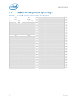
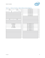
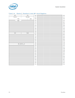
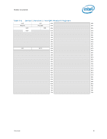
Register Description 2.2 16 Term Description RSVD Reserved Bits Reserved Registers Default Value upon a Reset "ST" appended to the end of a bit name Reserved Bit. This bit is reserved for future expansion and must not be written. The PCI Local Bus Specification, Revision 2.2 requires that reserved bits must be preserved. Any software that modifies a register that contains a reserved bit is responsible for reading the register, modifying the desired bits, and writing back the result. Some of the processor registers described in this section contain reserved bits. These bits are labeled "Reserved". Software must deal correctly with fields that are reserved. On reads, software must use appropriate masks to extract the defined bits and not rely on reserved bits being any particular value. On writes, software must ensure that the values of reserved bit positions are preserved. That is, the values of reserved bit positions must first be read, merged with the new values for other bit positions and then written back. Note that software does not need to perform a read-merge-write operation for the Configuration Address (CONFIG_ADDRESS) register. In addition to reserved bits within a register, the processor contains address locations in the configuration space that are marked either "Reserved" or "Intel Reserved". The processor responds to accesses to "Reserved" address locations by completing the host cycle. When a "Reserved" register location is read, a zero value is returned. ("Reserved" registers can be 8, 16, or 32 bits in size). Writes to "Reserved" registers have no effect on the processor. Registers that are marked as "Intel Reserved" must not be modified by system software. Writes to "Intel Reserved" registers may cause system failure. Reads to "Intel Reserved" registers may return a non-zero value. Upon a reset, the processor sets all of its internal configuration registers to predetermined default states. Some register values at reset are determined by external strapping options. The default state represents the minimum functionality feature set required to successfully bring up the system. Hence, it does not represent the optimal system configuration. It is the responsibility of the system initialization software (usually BIOS) to properly determine the DRAM configurations, operating parameters and optional system features that are applicable, and to program the processor registers accordingly. The bit is "sticky" or unchanged by a hard reset. These bits can only be cleared by a PWRGOOD reset. Platform Configuration Structure The processor contains 6 PCI devices within a single physical component. The configuration registers for these devices are mapped as devices residing on the PCI bus assigned for the processor socket. Bus number is derived by the max bus range setting and processor socket number. • Device 0: Generic processor non-core. Device 0, Function 0 contains the generic non-core configuration registers for the processor and resides at DID (Device ID) of 2C41h. Device 0, Function 1 contains the System Address Decode registers and resides at DID of 2C01h. • Device 2: Intel QPI. Device 2, Function 0 contains the Intel® QuickPath Interconnect configuration registers for Intel QPI Link 0 and resides at DID of 2C10h. Device 2, Function 1 contains the physical layer registers for Intel QPI Link 0 and resides at DID of 2C11h. • Device 3: Integrated Memory Controller. Device 3, Function 0 contains the general registers for the Integrated Memory Controller and resides at DID of 2C18h. Device 3, Function 1 contains the Target Address Decode registers for the Integrated Memory Controller and resides at DID of 2C19h. Device 3, Function 2 contains the RAS registers for the Integrated Memory Controller and resides at DID of 2C1Ah. Device 3, Function 4 contains the test registers for the Integrated Memory Controller and resides at DID of 2C1Ch. Function 2 only applies to processors supporting registered DIMMs. • Device 4: Integrated Memory Controller Channel 0. Device 4, Function 0 contains the control registers for Integrated Memory Controller Channel 0 and resides at DID of 2C20h. Device 4, Function 1 contains the address registers for Integrated Memory Controller Channel 0 and resides at DID of 2C21h. Device 4, Function 2 contains the rank registers for Integrated Memory Controller Channel 0 and resides Datasheet
-
 1
1 -
2
-
3
-
4
-
5
-
6
-
7
-
8
-
9
-
10
-
 11
11 -
 12
12 -
 13
13 -
 14
14 -
 15
15 -
 16
16 -
 17
17 -
 18
18 -
 19
19 -
 20
20 -
 21
21 -
22
-
23
-
24
-
25
-
26
-
27
-
28
-
29
-
30
-
31
-
32
-
33
-
34
-
35
-
36
-
37
-
38
-
39
-
40
-
41
-
42
-
43
-
44
-
45
-
46
-
47
-
48
-
49
-
50
-
51
-
52
-
53
-
54
-
55
-
56
-
57
-
58
-
59
-
60
-
61
-
62
-
63
-
64
-
65
-
66
-
67
-
68
-
69
-
70
-
71
-
72
-
73
-
74
-
75
-
76
-
77
-
78
-
79
-
80
-
81
-
82
-
83
-
84
-
85
-
86
-
87
-
88
-
89
-
90
-
91
-
92
-
93
-
94
-
95
-
96
-
97
-
98
 |
 |