Intel BX80605I7870 Data Sheet - Page 89
MC_RIR_WAY_CH0_12, MC_RIR_WAY_CH0_13
 |
UPC - 735858210461
View all Intel BX80605I7870 manuals
Add to My Manuals
Save this manual to your list of manuals |
Page 89 highlights
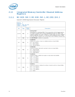
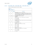
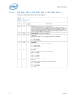
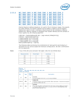
Register Description 2.12.2 MC_RIR_WAY_CH0_0, MC_RIR_WAY_CH0_1 MC_RIR_WAY_CH0_2, MC_RIR_WAY_CH0_3 MC_RIR_WAY_CH0_4, MC_RIR_WAY_CH0_5 MC_RIR_WAY_CH0_6, MC_RIR_WAY_CH0_7 MC_RIR_WAY_CH0_8, MC_RIR_WAY_CH0_9 MC_RIR_WAY_CH0_10, MC_RIR_WAY_CH0_11 MC_RIR_WAY_CH0_12, MC_RIR_WAY_CH0_13 MC_RIR_WAY_CH0_14, MC_RIR_WAY_CH0_15 MC_RIR_WAY_CH0_16, MC_RIR_WAY_CH0_17 MC_RIR_WAY_CH0_18, MC_RIR_WAY_CH0_19 MC_RIR_WAY_CH0_20, MC_RIR_WAY_CH0_21 MC_RIR_WAY_CH0_22, MC_RIR_WAY_CH0_23 MC_RIR_WAY_CH0_24, MC_RIR_WAY_CH0_25 MC_RIR_WAY_CH0_26, MC_RIR_WAY_CH0_27 MC_RIR_WAY_CH0_28, MC_RIR_WAY_CH0_29 MC_RIR_WAY_CH0_30, MC_RIR_WAY_CH0_31 Channel Rank Interleave Way Range Registers. These registers allow the user to define the ranks and offsets that apply to the ranges defined by the LIMIT in the MC_RIR_LIMIT_CH registers. The mappings are as follows: RIR_LIMIT_CH{chan}[0] -> RIR_WAY_CH{chan}[3:0] RIR_LIMIT_CH{chan}[1] -> RIR_WAY_CH{chan}[7:6] RIR_LIMIT_CH{chan}[2] -> RIR_WAY_CH{chan}[11:10] RIR_LIMIT_CH{chan}[3] -> RIR_WAY_CH{chan}[15:14] RIR_LIMIT_CH{chan}[4] -> RIR_WAY_CH{chan}[19:18] RIR_LIMIT_CH{chan}[5] -> RIR_WAY_CH{chan}[23:22] RIR_LIMIT_CH{chan}[6] -> RIR_WAY_CH{chan}[27:26] RIR_LIMIT_CH{chan}[7] -> RIR_WAY_CH{chan}[31:28] Device: 4 Function: 2 Offset: 80h, 84h, 88h, 8Ch, 90h, 94h, 98h, 9Ch, A0h, A4h, A8h, ACh, B0h, B4h, B8h, BCh, C0h, C4h, C8h, CCh, D0h, D4h, D8h, DCh, E0h, E4h, E8h, ECh, F0h, F4h, F8h, FCh Access as a Dword Bit 13:4 3:0 Type RW RW Reset Value Description 0 OFFSET. This field defines the offset used in the rank interleave. This is a 2's complement value. 0 RANK. This field defines which rank participates in WAY(n). If MC.CLOSEDPAGE=1, this field defines the DRAM rank selected when MemoryAddress[7:6]=(n). If MC.CLOSEDPAGE=0, this field defines which rank is selected when MemoryAddress[13:12]=(n). (n) is the instantiation of the register. This field is organized by physical rank. Bits [3:2] are the encoded DIMM ID(slot). Bits [1:0] are the rank within that DIMM. Datasheet 89
-
 1
1 -
2
-
3
-
4
-
5
-
6
-
7
-
8
-
9
-
10
-
11
-
12
-
13
-
14
-
15
-
16
-
17
-
18
-
19
-
20
-
21
-
22
-
23
-
24
-
25
-
26
-
27
-
28
-
29
-
30
-
31
-
32
-
33
-
34
-
35
-
36
-
37
-
38
-
39
-
40
-
41
-
42
-
43
-
44
-
45
-
46
-
47
-
48
-
49
-
50
-
51
-
52
-
53
-
54
-
55
-
56
-
57
-
58
-
59
-
60
-
61
-
62
-
63
-
64
-
65
-
66
-
67
-
68
-
69
-
70
-
71
-
72
-
73
-
74
-
75
-
76
-
77
-
78
-
79
-
80
-
81
-
82
-
83
-
 84
84 -
 85
85 -
 86
86 -
 87
87 -
 88
88 -
 89
89 -
 90
90 -
 91
91 -
 92
92 -
 93
93 -
 94
94 -
95
-
96
-
97
-
98
 |
 |
