Intel BX80605I7870 Data Sheet - Page 45
Sad_pciexbar, Sad_dram_rule_0, Sad_dram_rule_1, Sad_dram_rule_2, Sad_dram_rule_3, Sad_dram_rule_4,
 |
UPC - 735858210461
View all Intel BX80605I7870 manuals
Add to My Manuals
Save this manual to your list of manuals |
Page 45 highlights
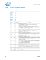
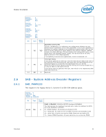
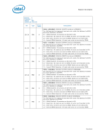
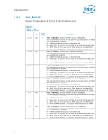
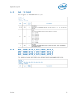
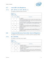
Register Description 2.6.5 2.6.6 SAD_PCIEXBAR Global register for PCIEXBAR address space. Device: 0 Function: 1 Offset: 50h Access as a Qword Bit Type 39:20 RW 3:1 RW 0 RW Reset Value Description ADDRESS. 0 Base address of PCIEXBAR. Must be naturally aligned to size; low order bits are ignored. SIZE. Size of the PCIEXBAR address space. (MAX bus number). 000 = 256 MB. 001 = Reserved. 010 = Reserved. 0 011 = Reserved. 100 = Reserved. 101 = Reserved. 110 = 64 MB. 111 = 128 MB. ENABLE. 0 Enable for PCIEXBAR address space. Editing size should not be done without also enabling range. SAD_DRAM_RULE_0, SAD_DRAM_RULE_1, SAD_DRAM_RULE_2, SAD_DRAM_RULE_3 SAD_DRAM_RULE_4, SAD_DRAM_RULE_5 SAD_DRAM_RULE_6, SAD_DRAM_RULE_7 This register provides SAD DRAM rules. Address Map for package determination. Device: 0 Function: 1 Offset: 80h, 84h, 88h, 8Ch, 90h, 94h, 98h, 9Ch Access as a Dword Bit Type Reset Value Description Datasheet 45
-
 1
1 -
2
-
3
-
4
-
5
-
6
-
7
-
8
-
9
-
10
-
11
-
12
-
13
-
14
-
15
-
16
-
17
-
18
-
19
-
20
-
21
-
22
-
23
-
24
-
25
-
26
-
27
-
28
-
29
-
30
-
31
-
32
-
33
-
34
-
35
-
36
-
37
-
38
-
39
-
 40
40 -
 41
41 -
 42
42 -
 43
43 -
 44
44 -
 45
45 -
 46
46 -
 47
47 -
 48
48 -
 49
49 -
 50
50 -
51
-
52
-
53
-
54
-
55
-
56
-
57
-
58
-
59
-
60
-
61
-
62
-
63
-
64
-
65
-
66
-
67
-
68
-
69
-
70
-
71
-
72
-
73
-
74
-
75
-
76
-
77
-
78
-
79
-
80
-
81
-
82
-
83
-
84
-
85
-
86
-
87
-
88
-
89
-
90
-
91
-
92
-
93
-
94
-
95
-
96
-
97
-
98
 |
 |
