Intel BX80605I7870 Data Sheet - Page 39
PCICMD - Command Register
 |
UPC - 735858210461
View all Intel BX80605I7870 manuals
Add to My Manuals
Save this manual to your list of manuals |
Page 39 highlights
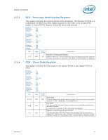
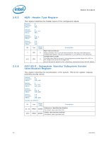
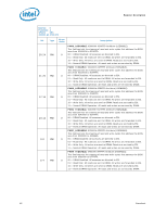
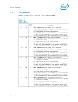
Register Description 2.5.7 PCICMD - Command Register This register defines the PCI 3.0 compatible command register values applicable to PCI Express space. Device: Function: Offset: 0 0-1 04h Device: Function: Offset: 2 0-1, 4-5 04h Device: Function: Offset: 3 0-2, 4 04h Device: Function: Offset: 4-6 0-3 04h Bit 15:11 10 9 8 7 6 5 4 3 2 1 0 Type RV RO RO RO RO RO RO RO RO RO RO RO Reset Value 0 0 0 0 0 0 0 0 0 1 1 0 Description Reserved. (by PCI SIG) INTxDisable: Interrupt Disable Controls the ability of the PCI Express port to generate INTx messages. If this device does not generate interrupts then this bit is not implemented and is RO. If this device generates interrupts then this bit is RW and this bit disables the device/function from asserting INTx#. A value of 0 enables the assertion of its INTx# signal. A value of 1 disables the assertion of its INTx# signal. 1 = Legacy Interrupt mode is disabled 0 = Legacy Interrupt mode is enabled FB2B: Fast Back-to-Back Enable This bit controls whether or not the master can do fast back-to-back writes. Since this device is strictly a target this bit is not implemented. This bit is hardwired to 0. Writes to this bit position have no effect. SERRE: SERR Message Enable This bit is a global enable bit for this devices SERR messaging. This host bridge will not implement SERR messaging. This bit is hardwired to 0. If SERR is used for error generation, then this bit must be RW and enable/disable SERR signaling. IDSELWCC: IDSEL Stepping/Wait Cycle Control Per PCI 2.3 specification this bit is hardwired to 0. PERRE: Parity Error Response Enable Parity error is not implemented in this host bridge. This bit is hardwired to 0. VGAPSE: VGA palette snoop Enable This host bridge does not implement this bit. This bit is hardwired to 0. MWIEN: Memory Write and Invalidate Enable This host bridge will never issue memory write and invalidate commands. This bit is therefore hardwired to 0. SCE: Special Cycle Enable This host bridge does not implement this bit. This bit is hardwired to a 0. BME: Bus Master Enable This host bridge is always enabled as a master. This bit is hardwired to a 1. MSE: Memory Space Enable This host bridge always allows access to main memory. This bit is not implemented and is hardwired to 1. IOAE: Access Enable This bit is not implemented in this host bridge and is hardwired to 0. Datasheet 39
-
 1
1 -
2
-
3
-
4
-
5
-
6
-
7
-
8
-
9
-
10
-
11
-
12
-
13
-
14
-
15
-
16
-
17
-
18
-
19
-
20
-
21
-
22
-
23
-
24
-
25
-
26
-
27
-
28
-
29
-
30
-
31
-
32
-
33
-
 34
34 -
 35
35 -
 36
36 -
 37
37 -
 38
38 -
 39
39 -
 40
40 -
 41
41 -
 42
42 -
 43
43 -
 44
44 -
45
-
46
-
47
-
48
-
49
-
50
-
51
-
52
-
53
-
54
-
55
-
56
-
57
-
58
-
59
-
60
-
61
-
62
-
63
-
64
-
65
-
66
-
67
-
68
-
69
-
70
-
71
-
72
-
73
-
74
-
75
-
76
-
77
-
78
-
79
-
80
-
81
-
82
-
83
-
84
-
85
-
86
-
87
-
88
-
89
-
90
-
91
-
92
-
93
-
94
-
95
-
96
-
97
-
98
 |
 |
