Intel BX80605I7870 Data Sheet - Page 15
Register Description
 |
UPC - 735858210461
View all Intel BX80605I7870 manuals
Add to My Manuals
Save this manual to your list of manuals |
Page 15 highlights
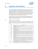
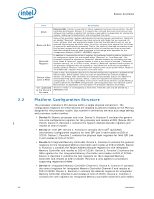
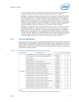
Register Description 2 Register Description 2.1 i The processor supports PCI configuration space accesses using the mechanism denoted as Configuration Mechanism in the PCI specification as defined in the PCI Local Bus Specification, Revision 2.3, as well as the PCI Express* enhanced configuration mechanism as specified in the PCI Express Base Specification, Revision 1.1. All the registers are organized by bus, device, function, etc. as defined in the PCI Express Base Specification, Revision 1.1. All processor registers appear on the PCI bus assigned for the processor socket. Bus number is derived by the max bus range setting and processor socket number. All multi-byte numeric fields use "little-endian" ordering (i.e., lower addresses contain the least significant parts of the field). As processor features vary by component, not all of the register descriptions in this document apply to all processors. This document highlights registers which do not apply to all processor components. Refer to the particular processor's Specification Update for a list of features supported. Register Terminology Registers and register bits are assigned one or more of the following attributes. These attributes define the behavior of register and the bit(s) that are contained with in. All bits are set to default values by hard reset. Sticky bits retain their states between hard resets. Term RO WO RW RC RCW RW1C RW0C RW1S RW0S RWL RWO RRW L Description Read Only. If a register bit is read only, the hardware sets its state. The bit may be read by software. Writes to this bit have no effect. Write Only. The register bit is not implemented as a bit. The write causes some hardware event to take place. Read/Write. A register bit with this attribute can be read and written by software. Read Clear: The bit or bits can be read by software, but the act of reading causes the value to be cleared. Read Clear/Write: A register bit with this attribute will get cleared after the read. The register bit can be written. Read/Write 1 Clear. A register bit with this attribute can be read or cleared by software. In order to clear this bit, a one must be written to it. Writing a zero will have no effect. Read/Write 0 Clear. A register bit with this attribute can be read or cleared by software. In order to clear this bit, a zero must be written to it. Writing a one will have no effect. Read/Write 1 Set: A register bit can be either read or set by software. In order to set this bit, a one must be written to it. Writing a zero to this bit has no effect. Hardware will clear this bit. Read/Write 0 Set: A register bit can be either read or set by software. In order to set this bit, a zero must be written to it. Writing a one to this bit has no effect. Hardware will clear this bit. Read/Write/Lock. A register bit with this attribute can be read or written by software. Hardware or a configuration bit can lock the bit and prevent it from being updated. Read/Write Once. A register bit with this attribute can be written to only once after power up. After the first write, the bit becomes read only. This attribute is applied on a bit by bit basis. For example, if the RWO attribute is applied to a 2 bit field, and only one bit is written, then the written bit cannot be rewritten (unless reset). The unwritten bit, of the field, may still be written once. This is special case of RWL. Read/Restricted Write. This bit can be read and written by software. However, only supported values will be written. Writes of non supported values will have no effect. Lock. A register bit with this attribute becomes Read Only after a lock bit is set. Datasheet 15
-
 1
1 -
2
-
3
-
4
-
5
-
6
-
7
-
8
-
9
-
 10
10 -
 11
11 -
 12
12 -
 13
13 -
 14
14 -
 15
15 -
 16
16 -
 17
17 -
 18
18 -
 19
19 -
 20
20 -
21
-
22
-
23
-
24
-
25
-
26
-
27
-
28
-
29
-
30
-
31
-
32
-
33
-
34
-
35
-
36
-
37
-
38
-
39
-
40
-
41
-
42
-
43
-
44
-
45
-
46
-
47
-
48
-
49
-
50
-
51
-
52
-
53
-
54
-
55
-
56
-
57
-
58
-
59
-
60
-
61
-
62
-
63
-
64
-
65
-
66
-
67
-
68
-
69
-
70
-
71
-
72
-
73
-
74
-
75
-
76
-
77
-
78
-
79
-
80
-
81
-
82
-
83
-
84
-
85
-
86
-
87
-
88
-
89
-
90
-
91
-
92
-
93
-
94
-
95
-
96
-
97
-
98
 |
 |