Intel BX80605I7870 Data Sheet - Page 44
Sad_hen, Sad_smram
 |
UPC - 735858210461
View all Intel BX80605I7870 manuals
Add to My Manuals
Save this manual to your list of manuals |
Page 44 highlights
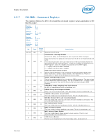
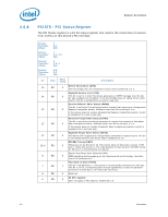
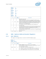
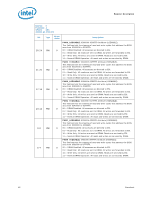
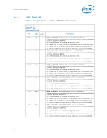
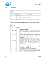
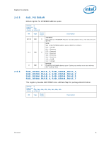
Register Description 2.6.3 2.6.4 SAD_HEN Register for legacy Hole Enable. Device: 0 Function: 1 Offset: 48h Access as a Dword Bit Type Reset Value Description 7 RW 0 HEN: Hole Enable This field enables a memory hole in DRAM space. The DRAM that lies "behind" this space is not remapped. 0 = No Memory hole. 1 = Memory hole from 15 MB to 16 MB. SAD_SMRAM Register for legacy 9Dh address space. Note both IOH and non-core have this now. Device: 0 Function: 1 Offset: 4Ch Access as a Dword Bit 14 13 12 11 10:8 Type RW RW RW1S RW RO Reset Value Description SMM Space Open (D_OPEN) When D_OPEN=1 and D_LCK=0, the SMM space DRAM is made visible even 0 when SMM decode is not active. This is intended to help BIOS initialize SMM space. Software should ensure that D_OPEN=1 and D_CLS=1 are not set at the same time. SMM Space Closed (D_CLS) When D_CLS = 1 SMM space DRAM is not accessible to data references, even 0 if SMM decode is active. Code references may still access SMM space DRAM. This will allow SMM software to reference through SMM space to update the display even when SMM is mapped over the VGA range. Software should ensure that D_OPEN=1 and D_CLS=1 are not set at the same time. SMM Space Locked (D_LCK) When D_LCK is set to 1 then D_OPEN is reset to 0 and D_LCK, D_OPEN, C_BASE_SEG, G_SMRAME, PCIEXBAR, (DRAM_RULEs and INTERLEAVE_LISTs) become read only. D_LCK can be set to 1 via a normal configuration space write but can only be cleared by a Reset. The 0 combination of D_LCK and D_OPEN provide convenience with security. The BIOS can use the D_OPEN function to initialize SMM space and then use D_LCK to "lock down" SMM space in the future so that no application software (or BIOS itself) can violate the integrity of SMM space, even if the program has knowledge of the D_OPEN function. Note that TAD does not implement this lock. Global SMRAM Enable (G_SMRAME) If set to a 1, then Compatible SMRAM functions are enabled, providing 128 0 KB of DRAM accessible at the A0000h address while in SMM (ADSB with SMM decode). To enable Extended SMRAM function this bit has to be set to 1. Once D_LCK is set, this bit becomes read only. Compatible SMM Space Base Segment (C_BASE_SEG) This field indicates the location of SMM space. SMM DRAM is not remapped. It - is simply made visible if the conditions are right to access SMM space, otherwise the access is forwarded to HI. Only SMM space between A0000h and BFFFFh is supported so this field is hardwired to 010. 44 Datasheet
-
 1
1 -
2
-
3
-
4
-
5
-
6
-
7
-
8
-
9
-
10
-
11
-
12
-
13
-
14
-
15
-
16
-
17
-
18
-
19
-
20
-
21
-
22
-
23
-
24
-
25
-
26
-
27
-
28
-
29
-
30
-
31
-
32
-
33
-
34
-
35
-
36
-
37
-
38
-
 39
39 -
 40
40 -
 41
41 -
 42
42 -
 43
43 -
 44
44 -
 45
45 -
 46
46 -
 47
47 -
 48
48 -
 49
49 -
50
-
51
-
52
-
53
-
54
-
55
-
56
-
57
-
58
-
59
-
60
-
61
-
62
-
63
-
64
-
65
-
66
-
67
-
68
-
69
-
70
-
71
-
72
-
73
-
74
-
75
-
76
-
77
-
78
-
79
-
80
-
81
-
82
-
83
-
84
-
85
-
86
-
87
-
88
-
89
-
90
-
91
-
92
-
93
-
94
-
95
-
96
-
97
-
98
 |
 |