Intel BX80605I7870 Data Sheet - Page 47
Intel QPI Link Registers, Integrated Memory Controller Control Registers
 |
UPC - 735858210461
View all Intel BX80605I7870 manuals
Add to My Manuals
Save this manual to your list of manuals |
Page 47 highlights
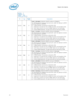
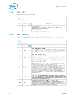
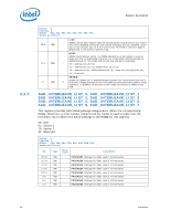
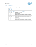
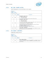
Register Description 2.7 2.7.1 2.8 2.8.1 Intel QPI Link Registers QPI_QPILCL_L0, QPI_QPILCL_L1 This register provides Intel QPI Link Control. Device: 2 Function: 0, 4 Offset: 48h Access as a Dword Bit Type Reset Value Description 21 RW 20 RW 18 RW L1_MASTER Indicates that this end of the link is the L1 master. This link transmitter bit is an L1 power state master and can initiate an L1 power state transition. If this bit is 0 not set, then the link transmitter is an L1 power state slave and should respond to L1 transitions with an ACK or NACK. If the link power state of L1 is enabled, then there is one master and one slave per link. The master may only issue single L1 requests, while the slave can only issue single L1_Ack or L1_NAck responses for the corresponding request. L1_ENABLE Enables L1 mode at the transmitter. This bit should be ANDed with the receive 0 L1 capability bit received during parameter exchange to determine if a transmitter is allowed to enter into L1. This is NOT a bit that determines the capability of a device. L0S_ENABLE Enables L0s mode at the transmitter. This bit should be ANDed with the receive 0 L0s capability bit received during parameter exchange to determine if a transmitter is allowed to enter into L0s. This is NOT a bit that determines the capability of a device. Integrated Memory Controller Control Registers The registers in this section apply only to processors supporting registered DIMMs. MC_CONTROL This register is the Primary control register. Device: 3 Function: 0 Offset: 48h Access as a Dword Bit Type Reset Value Description CHANNEL2_ACTIVE 10 RW 0 When set, indicates MC channel 2 is active. This bit is controlled (set/reset) by software only. This bit is required to be set for any active channel when INIT_DONE is set by software. CHANNEL1_ACTIVE When set, indicates MC channel 1 is active. This bit is controlled (set/reset) 9 RW 0 by software only. This bit is required to be set for any active channel when INIT_DONE is set by software. Channel 0 AND Channel 1 active must both be set for a lockstep or mirrored pair. Datasheet 47
-
 1
1 -
2
-
3
-
4
-
5
-
6
-
7
-
8
-
9
-
10
-
11
-
12
-
13
-
14
-
15
-
16
-
17
-
18
-
19
-
20
-
21
-
22
-
23
-
24
-
25
-
26
-
27
-
28
-
29
-
30
-
31
-
32
-
33
-
34
-
35
-
36
-
37
-
38
-
39
-
40
-
41
-
 42
42 -
 43
43 -
 44
44 -
 45
45 -
 46
46 -
 47
47 -
 48
48 -
 49
49 -
 50
50 -
 51
51 -
 52
52 -
53
-
54
-
55
-
56
-
57
-
58
-
59
-
60
-
61
-
62
-
63
-
64
-
65
-
66
-
67
-
68
-
69
-
70
-
71
-
72
-
73
-
74
-
75
-
76
-
77
-
78
-
79
-
80
-
81
-
82
-
83
-
84
-
85
-
86
-
87
-
88
-
89
-
90
-
91
-
92
-
93
-
94
-
95
-
96
-
97
-
98
 |
 |