Intel BX80605I7870 Data Sheet - Page 41
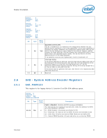
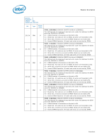
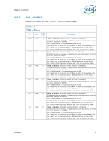
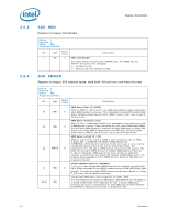
SAD - System Address Decoder Registers
 |
UPC - 735858210461
View all Intel BX80605I7870 manuals
Add to My Manuals
Save this manual to your list of manuals |
Page 41 highlights
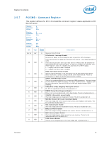
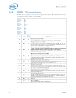
Register Description Device: Function: Offset: Device: Function: Offset: Device: Function: Offset: Device: Function: Offset: 0 0-1 06h 2 0-1, 4-5 06h 3 0-2, 4 06h 4-6 0-3 06h Bit Type Reset Value Description Capability List (CLIST) This bit is hardwired to 1 to indicate to the configuration software that this device/function implements a list of new capabilities. A list of new capabilities is accessed via registers CAPPTR at the configuration address offset 34h from the 4 RO TBD start of the PCI configuration space header of this function. Register CAPPTR contains the offset pointing to the start address with configuration space of this device where the capability register resides. This bit must be set for a PCI Express device or if the VSEC capability. If no capability structures are implemented, this bit is hardwired to 0. Interrupt Status If this device generates an interrupt, then this read-only bit reflects the state of the interrupt in the device/function. Only when the Interrupt Disable bit in the 3 RO 0 command register is a 0 and this Interrupt Status bit is a 1, will the device's/function's INTx# signal be asserted. Setting the Interrupt Disable bit to a 1 has no effect on the state of this bit. If this device does not generate interrupts, then this bit is not implemented (RO and reads returns 0). 2:0 RO 0 Reserved 2.6 2.6.1 SAD - System Address Decoder Registers SAD_PAM0123 This register is for legacy device 0, function 0 at 90h-93h address space. Device: 0 Function: 1 Offset: 40h Access as a Dword Bit Type 29:28 RW Reset Value Description PAM3_HIENABLE. 0D4000h-0D7FFFh Attribute (HIENABLE). This field controls the steering of read and write cycles that address the BIOS area from 0D4000h to 0D7FFFh. 0 00 =DRAM Disabled: All accesses are directed to ESI. 01 = Read Only: All reads are sent to DRAM. All writes are forwarded to ESI. 10 = Write Only: All writes are send to DRAM. Reads are serviced by ESI. 11 = Normal DRAM Operation: All reads and writes are serviced by DRAM. Datasheet 41
-
 1
1 -
2
-
3
-
4
-
5
-
6
-
7
-
8
-
9
-
10
-
11
-
12
-
13
-
14
-
15
-
16
-
17
-
18
-
19
-
20
-
21
-
22
-
23
-
24
-
25
-
26
-
27
-
28
-
29
-
30
-
31
-
32
-
33
-
34
-
35
-
 36
36 -
 37
37 -
 38
38 -
 39
39 -
 40
40 -
 41
41 -
 42
42 -
 43
43 -
 44
44 -
 45
45 -
 46
46 -
47
-
48
-
49
-
50
-
51
-
52
-
53
-
54
-
55
-
56
-
57
-
58
-
59
-
60
-
61
-
62
-
63
-
64
-
65
-
66
-
67
-
68
-
69
-
70
-
71
-
72
-
73
-
74
-
75
-
76
-
77
-
78
-
79
-
80
-
81
-
82
-
83
-
84
-
85
-
86
-
87
-
88
-
89
-
90
-
91
-
92
-
93
-
94
-
95
-
96
-
97
-
98
 |
 |