HP Superdome SX2000 User Service Guide, Seventh Edition - HP Integrity Superdo - Page 33
Memory Controller, DIMM Architecture, Memory Interconnect
 |
View all HP Superdome SX2000 manuals
Add to My Manuals
Save this manual to your list of manuals |
Page 33 highlights
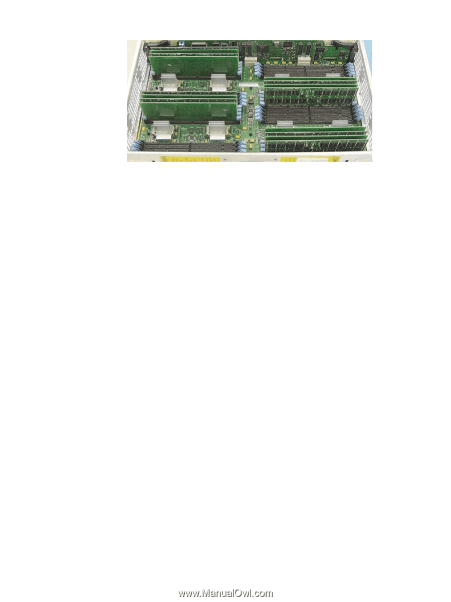
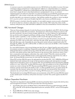
Figure 1-10 Cell Memory DIMMs are named according to both physical location and loading order. The physical location is used for connectivity on the board and is the same for all quads. Physical location is a letter (A or B) followed by a number (0, 1, 2, or 3). The letter indicates which side of the quad the DIMM is on. A is the left side, or the side nearest CC. The DIMMs are then numbered 0 through 3, starting at the outer DIMM and moving inwards the memory controllers. Memory Controller The memory controller CEC's primary function is to source address and control signals and multiplex and demultiplex data between the CC and the devices on the DDR DIMMs. Four independent memory blocks, consisting of two memory controllers and eight DIMMs, are supported by interface buses running between the CC and the memory controller. The memory controller converts these link streams to the correct signaling voltage levels (1.8 V) and timing for DDR2 protocol. Bandwidth is limited by the memory interface buses that transfer data between the CC and the memory controller. The memory controller also performs the write (tag update) portion of a read-modify-write (RMW) access. The memory controller is bit sliced, and two controllers are required to form one 72-bit CC memory interface data (MID) bus. The CC MID buses are bidirectional, source synchronous, and run at 533.33 MT/s. The memory side of a pair of memory controller ASICs consists of two 144-bit bidirectional DDR2 SDRAM data buses operating at 533.33 MT/s. Each bus supports up to four echelons of DRAMs. DIMM Architecture The fundamental building block of the DIMM is a DDR2 DRAM with a 4-bit data width. Each DIMM transfers 72 bits of data on a read/write, and the data is double-clocked at a clock frequency of 266.67 MHz for an effective peak transfer rate of 533.33 MT/s. Each DIMM includes 36 DRAM devices for data storage and two identical custom address buffers. These buffers fan out and check the parity of address and control signals received from the memory controller. The DIMM densities for the sx2000 are 1 GB (256 Gb DRAMs), 2 GB (512 Gb DRAMs), and 4 GB (1 Gb DRAMs). The new sx2000 chipset DIMMs have the same mechanical form factor as the DIMMs used in Integrity systems, but the DIMM and the connector, are keyed differently from previous DIMM designs to prevent improper installation. The DIMM is roughly twice the height of an industry-standard DIMM. This height increase enables the DIMM to accommodate twice as many DRAMs as an industry-standard DIMM and provides redundant address and control signal contacts not available on industry-standard DDR2 DIMMs. Memory Interconnect MID bus data is transmitted through the four 72-bit, ECC-protected MID buses, each with a clock frequency equal to the CC core frequency. The data is transmitted on both edges of the clock, so the data transfer rate (533 MT/s) of each MID is twice the MID clock frequency (267 MHz). A CPUs and Memories 33
-
 1
1 -
2
-
3
-
4
-
5
-
6
-
7
-
8
-
9
-
10
-
11
-
12
-
13
-
14
-
15
-
16
-
17
-
18
-
19
-
20
-
21
-
22
-
23
-
24
-
25
-
26
-
27
-
 28
28 -
 29
29 -
 30
30 -
 31
31 -
 32
32 -
 33
33 -
 34
34 -
 35
35 -
 36
36 -
 37
37 -
 38
38 -
39
-
40
-
41
-
42
-
43
-
44
-
45
-
46
-
47
-
48
-
49
-
50
-
51
-
52
-
53
-
54
-
55
-
56
-
57
-
58
-
59
-
60
-
61
-
62
-
63
-
64
-
65
-
66
-
67
-
68
-
69
-
70
-
71
-
72
-
73
-
74
-
75
-
76
-
77
-
78
-
79
-
80
-
81
-
82
-
83
-
84
-
85
-
86
-
87
-
88
-
89
-
90
-
91
-
92
-
93
-
94
-
95
-
96
-
97
-
98
-
99
-
100
-
101
-
102
-
103
-
104
-
105
-
106
-
107
-
108
-
109
-
110
-
111
-
112
-
113
-
114
-
115
-
116
-
117
-
118
-
119
-
120
-
121
-
122
-
123
-
124
-
125
-
126
-
127
-
128
-
129
-
130
-
131
-
132
-
133
-
134
-
135
-
136
-
137
-
138
-
139
-
140
-
141
-
142
-
143
-
144
-
145
-
146
-
147
-
148
-
149
-
150
-
151
-
152
-
153
-
154
-
155
-
156
-
157
-
158
-
159
-
160
-
161
-
162
-
163
-
164
-
165
-
166
-
167
-
168
-
169
-
170
-
171
-
172
-
173
-
174
-
175
-
176
-
177
-
178
-
179
-
180
-
181
-
182
-
183
-
184
-
185
-
186
-
187
-
188
-
189
-
190
-
191
-
192
-
193
-
194
-
195
-
196
-
197
-
198
-
199
-
200
 |
 |