HP Superdome SX2000 User Service Guide, Seventh Edition - HP Integrity Superdo - Page 35
Cell Map, Link Interleaving, Memory Error Protection
 |
View all HP Superdome SX2000 manuals
Add to My Manuals
Save this manual to your list of manuals |
Page 35 highlights
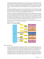
The 16 echelons in the memory subsystem can be subdivided into four independent memory quadrants accessed by four independent MID buses. Each quadrant contains two independent SDRAM buses. Four echelons can be installed on each SDRAM bus. The CC contains four MBATs, one for each memory quadrant. Each MBAT contains eight sets of routing CSRs (one per rank). Each routing CSR specifies the bits of the address that are masked or compared to select the corresponding rank, referred to as interleave bits. The routing CSR also specifies how the remaining address bits are routed to bank, row, and column address bits. To optimize bandwidth, consecutive memory accesses target echelons that are as far from each other as possible. For this reason, the interleaving algorithm programs the MBATs so that consecutive addresses target echelons in an order that skips first across quadrants, then across SDRAM buses, then across echelons per SDRAM bus, then across banks per rank. Cell Map Cell mapping creates a scheme that is easy to implement in hardware. It enables easy calculation of the interleaving parameters for software. In order to do this part of the physical address to perform a lookup into a table, it gives the actual physical cell and ways of interleaving into memory at this address. Be aware of the following: • A portion of memory that is being interleaved across must start at an offset that is a multiple of the memory chunk for that entry. For example, to interleave across 16 GB of memory with one entry, the starting address for this chunk must be 0 GB, 16 GB, 32 GB, 48 GB, or 64 GB. If using three 2 GB entries to interleave across three cells, then the multiple must be 2 GB, not 6 GB. • Interleaving is performed across the actual cells within the system. Interleaving can be done across a minimum of 0.5 GB on a cell, and a maximum interleave across 256 GB per cell. • Each cell in an interleave group must have the same amount of memory interleaved. That is, you cannot interleave 2 GB in one cell and 4 GB in another cell. The cell map remains the same size as in previous HP Integrity CECs. Link Interleaving The link interleaving functionality did not exist in sx1000. This logic is new for the sx2000 CC. The sx2000 enables cells to be connected through multiple paths. In particular, each CC chip has three crossbar links. When one CC sends a packet to another CC, it must specify which link to use. The CC is the sx2000 chipset cell controller. It interfaces to processors, main memory, the crossbar fabric, an I/O subsystem, and processor-dependent hardware (PDH). Two data path CPU bus interfaces are implemented, with support for up to four processors on each bus. The CC supports bus speeds of 200 MHz and 267 MHz. The 128-bit data bus is source synchronous, and data can be transferred at twice the bus frequency: 400 MT/s or 533 MT/s. The address bus is 50 bits wide, but only 44 bits are used by the CC. Error correction is provided on the data bus and parity protection is provided on the address bus. Memory Error Protection All of the CC cache lines are protected in memory by an error correction code (ECC). The sx2000 memory ECC scheme is significantly different from the sx1000 memory ECC scheme. An ECC code word is 288 bits long: 264 bits of payload (data and tag) and 24 bits of redundancy. An ECC code word is contained in each pair of 144-bit chunks. The first chunk in the pair (for example chunk 0 in the 0,1 pair) contains all the even nibbles of the payload and redundancy, and the second chunk contains all the odd nibbles. The memory data path (MDP) block checks for, and if necessary, corrects any correctable errors. CPUs and Memories 35
-
 1
1 -
2
-
3
-
4
-
5
-
6
-
7
-
8
-
9
-
10
-
11
-
12
-
13
-
14
-
15
-
16
-
17
-
18
-
19
-
20
-
21
-
22
-
23
-
24
-
25
-
26
-
27
-
28
-
29
-
 30
30 -
 31
31 -
 32
32 -
 33
33 -
 34
34 -
 35
35 -
 36
36 -
 37
37 -
 38
38 -
 39
39 -
 40
40 -
41
-
42
-
43
-
44
-
45
-
46
-
47
-
48
-
49
-
50
-
51
-
52
-
53
-
54
-
55
-
56
-
57
-
58
-
59
-
60
-
61
-
62
-
63
-
64
-
65
-
66
-
67
-
68
-
69
-
70
-
71
-
72
-
73
-
74
-
75
-
76
-
77
-
78
-
79
-
80
-
81
-
82
-
83
-
84
-
85
-
86
-
87
-
88
-
89
-
90
-
91
-
92
-
93
-
94
-
95
-
96
-
97
-
98
-
99
-
100
-
101
-
102
-
103
-
104
-
105
-
106
-
107
-
108
-
109
-
110
-
111
-
112
-
113
-
114
-
115
-
116
-
117
-
118
-
119
-
120
-
121
-
122
-
123
-
124
-
125
-
126
-
127
-
128
-
129
-
130
-
131
-
132
-
133
-
134
-
135
-
136
-
137
-
138
-
139
-
140
-
141
-
142
-
143
-
144
-
145
-
146
-
147
-
148
-
149
-
150
-
151
-
152
-
153
-
154
-
155
-
156
-
157
-
158
-
159
-
160
-
161
-
162
-
163
-
164
-
165
-
166
-
167
-
168
-
169
-
170
-
171
-
172
-
173
-
174
-
175
-
176
-
177
-
178
-
179
-
180
-
181
-
182
-
183
-
184
-
185
-
186
-
187
-
188
-
189
-
190
-
191
-
192
-
193
-
194
-
195
-
196
-
197
-
198
-
199
-
200
 |
 |