HP Superdome SX2000 User Service Guide, Seventh Edition - HP Integrity Superdo - Page 34
Mixing Different Sized DIMMs, Memory Interleaving, Memory Bank Attribute Table, MBAT across DIMMs
 |
View all HP Superdome SX2000 manuals
Add to My Manuals
Save this manual to your list of manuals |
Page 34 highlights
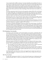
configuration of at least eight DIMMs (two in each quadrant) activates all four MID buses. The theoretical bandwidth of the memory subsystem can be calculated as follows: (533 MT/s * 8 Bytes/T * 4) = 17 GB/s The MID buses are bit-sliced across two memory controllers with 36-bits of data going to each memory controller. In turn, each memory controller takes that high-speed data (533 MT/s) from the MID, and combines four consecutive MID transfers to form one 144-bit DRAM bus. This DRAM bus is routed out in two 72-bit buses to two DIMM sets, which include four DIMMs each. The DDR DRAM bus runs at 267 MT/s and data is clocked on both edges of the clock. The DDR DRAM address and control (MIA) signals for each quadrant originate at the CC and are routed to the DIMMs through the memory controller. On previous systems, these signals did not touch the memory chips; they were routed to the DIMMs through fan out buffers. The DRAM address and control signals are protected by parity so that signaling errors are detected and do not cause silent data corruption. The MIA bus, comprised of the SDRAM address and control signals, is checked for parity by the memory controller. Each of the 32 DIMMs can generating a unique parity error signal that is routed to one of four parity error inputs per memory controller. Each memory controller then logically gates the DIMM parity error signals it receives with its own internal parity checks for the MIC and MIT buses. This logical gating results in a single parity error output that is driven to the CC and latched as an event in an internal memory-mapped register. Eight unique buses for command and control signals are transmitted from the CC to each memory controller simultaneously with the appropriate MID bus interconnect. Each MIC bus includes four signals running at 533 MT/s. Each command on the MIC bus takes four cycles to transmit and is protected by parity so that signaling errors are detected and do not cause silent data corruption. Four MIT buses are routed between the CC and the designated tag memory controllers. MIT buses run at 533 MT/s and use the same link type as the MID buses. Each MIT bus includes six signals and a differential strobe pair for deskewing. As with the MIA and MIC buses, the MIT is protected by parity so that signaling errors are detected and do not cause silent data corruption. Mixing Different Sized DIMMs Mixing different sized DIMMs is allowed, provided you follow these rules: • An echelon of DIMMs consists of two DIMMs of the same type. • All supported DIMM sizes can be present on a single cell board at the same time, provided previous rule is satisfied. • Memory must be added in one echelon increments. • The amount of memory contained in an interleaved group must be 2n bytes. Memory Interleaving Memory is interleaved in the following ways on sx2000 systems: • MBAT (across DIMMs) • Cell map (across cells) • Link (across fabrics) Memory Bank Attribute Table The memory bank attribute table (MBAT) interleaving is done on a per-cell basis before the partition is rendezvoused. The cell map and fabric interleaving are done after the partition has rendezvoused. SDRAM on the cell board is installed in physical units (echelons). The sx2000 has 16 independent echelons. Each echelon consists of two DDR DIMMs. Each rank can have multiple internal logical units called banks, and each bank contains multiple rows and columns of memory. An interleaving algorithm determines how a rank, bank, row, or column address is formed for a particular physical address. 34 Overview
-
 1
1 -
2
-
3
-
4
-
5
-
6
-
7
-
8
-
9
-
10
-
11
-
12
-
13
-
14
-
15
-
16
-
17
-
18
-
19
-
20
-
21
-
22
-
23
-
24
-
25
-
26
-
27
-
28
-
 29
29 -
 30
30 -
 31
31 -
 32
32 -
 33
33 -
 34
34 -
 35
35 -
 36
36 -
 37
37 -
 38
38 -
 39
39 -
40
-
41
-
42
-
43
-
44
-
45
-
46
-
47
-
48
-
49
-
50
-
51
-
52
-
53
-
54
-
55
-
56
-
57
-
58
-
59
-
60
-
61
-
62
-
63
-
64
-
65
-
66
-
67
-
68
-
69
-
70
-
71
-
72
-
73
-
74
-
75
-
76
-
77
-
78
-
79
-
80
-
81
-
82
-
83
-
84
-
85
-
86
-
87
-
88
-
89
-
90
-
91
-
92
-
93
-
94
-
95
-
96
-
97
-
98
-
99
-
100
-
101
-
102
-
103
-
104
-
105
-
106
-
107
-
108
-
109
-
110
-
111
-
112
-
113
-
114
-
115
-
116
-
117
-
118
-
119
-
120
-
121
-
122
-
123
-
124
-
125
-
126
-
127
-
128
-
129
-
130
-
131
-
132
-
133
-
134
-
135
-
136
-
137
-
138
-
139
-
140
-
141
-
142
-
143
-
144
-
145
-
146
-
147
-
148
-
149
-
150
-
151
-
152
-
153
-
154
-
155
-
156
-
157
-
158
-
159
-
160
-
161
-
162
-
163
-
164
-
165
-
166
-
167
-
168
-
169
-
170
-
171
-
172
-
173
-
174
-
175
-
176
-
177
-
178
-
179
-
180
-
181
-
182
-
183
-
184
-
185
-
186
-
187
-
188
-
189
-
190
-
191
-
192
-
193
-
194
-
195
-
196
-
197
-
198
-
199
-
200
 |
 |