Intel S1200BTL Product Specification - Page 126

Capacitive Loading, Closed-loop Stability, Common Mode Noise, Ripple/Noise, Timing Requirements

Page 126 highlights

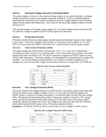
Design and Environmental Specifications Intel®Server Board S1200BT TPS Output +5 VSB ∆ Step Load Size (See note 2) 0.5 A Load Slew Rate 0.25 A/µsec Test capacitive Load 20 µF Note: Step loads on each 12 V output may happen simultaneously and should be tested that way. 10.3.6 Capacitive Loading The power supply is stable and meets all requirements with the following capacitive loading ranges. Table 50. Capacitve Loading Conditions Output +3.3 V +5 V +12 V -12 V +5 VSB Minimum 100 400 500 1 20 Maximum 2200 2200 2200 350 350 Units µF µF µF µF µF 10.3.7 Closed-loop Stability The power supply is unconditionally stable under all line/load/transient load conditions including capacitive load ranges. A minimum of 45°phase margin and -10 dB-gain margin is required. The power supply manufacturer provides proof of the unit's closed-loop stability with local sensing through the submission of Bode plots. Closed-loop stability is ensured at the maximum and minimum loads as applicable. 10.3.8 Common Mode Noise The Common Mode noise on any output does not exceed 350 mV pk-pk over the frequency band of 10 Hz to 20 MHz.  The measurement is made across a 100Ω resistor between each of the DC outputs, including ground, at the DC power connector and chassis ground (power subsystem enclosure).  The test setup uses a FET probe such as Tektronix* model P6046 or equivalent. 10.3.9 Ripple/Noise The maximum allowed ripple/noise output of the power supply is defined in the following table. This is measured over a bandwidth of 0 Hz to 20 MHz at the power supply output connectors. A 10 F tantalum capacitor is placed in parallel with a 0.1 F ceramic capacitor at the point of measurement. Table 51. Ripple and Noise +3.3 V 50 mVp-p +5 V 50 mVp-p +12 V 120 mVp-p -12 V 120 mVp-p +5 VSB 50 mVp-p 10.3.10 Timing Requirements The timing requirements for the power supply operation are as follows: 114 Revision 1.0 Intel order number G13326-003

  • 1
  • 2
  • 3
  • 4
  • 5
  • 6
  • 7
  • 8
  • 9
  • 10
  • 11
  • 12
  • 13
  • 14
  • 15
  • 16
  • 17
  • 18
  • 19
  • 20
  • 21
  • 22
  • 23
  • 24
  • 25
  • 26
  • 27
  • 28
  • 29
  • 30
  • 31
  • 32
  • 33
  • 34
  • 35
  • 36
  • 37
  • 38
  • 39
  • 40
  • 41
  • 42
  • 43
  • 44
  • 45
  • 46
  • 47
  • 48
  • 49
  • 50
  • 51
  • 52
  • 53
  • 54
  • 55
  • 56
  • 57
  • 58
  • 59
  • 60
  • 61
  • 62
  • 63
  • 64
  • 65
  • 66
  • 67
  • 68
  • 69
  • 70
  • 71
  • 72
  • 73
  • 74
  • 75
  • 76
  • 77
  • 78
  • 79
  • 80
  • 81
  • 82
  • 83
  • 84
  • 85
  • 86
  • 87
  • 88
  • 89
  • 90
  • 91
  • 92
  • 93
  • 94
  • 95
  • 96
  • 97
  • 98
  • 99
  • 100
  • 101
  • 102
  • 103
  • 104
  • 105
  • 106
  • 107
  • 108
  • 109
  • 110
  • 111
  • 112
  • 113
  • 114
  • 115
  • 116
  • 117
  • 118
  • 119
  • 120
  • 121
  • 122
  • 123
  • 124
  • 125
  • 126
  • 127
  • 128
  • 129
  • 130
  • 131
  • 132
  • 133
  • 134
  • 135
  • 136
  • 137
  • 138
  • 139
  • 140
  • 141
  • 142
  • 143
  • 144
  • 145
  • 146
  • 147
  • 148
  • 149
  • 150
  • 151
  • 152
  • 153

Design and Environmental Specifications
Intel®
Server Board S1200BT TPS
Revision 1.0
Intel order number G13326-003
114
Output
Step Load Size
(See note 2)
Load Slew Rate
Test capacitive Load
+5 VSB
0.5 A
0.25 A/μsec
20 μF
Note:
Step loads on each 12 V output may happen simultaneously and should be tested that way.
10.3.6
Capacitive Loading
The power supply is stable and meets all requirements with the following capacitive
loading ranges.
Table 50. Capacitve Loading Conditions
Output
Minimum
Maximum
Units
+3.3 V
100
2200
μF
+5 V
400
2200
μF
+12 V
500
2200
μF
-12 V
1
350
μF
+5 VSB
20
350
μF
10.3.7
Closed-loop Stability
The power supply is unconditionally stable under all line/load/transient load conditions including
capacitive load ranges. A minimum of 45°
phase margin and -10 dB-gain margin is required.
The power supply manufacturer provides proof of the unit‘s closed
-loop stability with local
sensing through the submission of Bode plots. Closed-loop stability is ensured at the maximum
and minimum loads as applicable.
10.3.8
Common Mode Noise
The Common Mode noise on any output does not exceed 350 mV pk-pk over the frequency
band of 10 Hz to 20 MHz.
The measurement is made across a 100Ω resistor between each of the DC outputs,
including ground, at the DC power connector and chassis ground (power subsystem
enclosure).
The test setup uses a FET probe such as Tektronix* model P6046 or equivalent.
10.3.9
Ripple/Noise
The maximum allowed ripple/noise output of the power supply is defined in the following table.
This is measured over a bandwidth of 0 Hz to 20 MHz at the power supply output connectors. A
10 F tantalum capacitor is placed in parallel with a 0.1 F ceramic capacitor at the point of
measurement.
Table 51. Ripple and Noise
+3.3 V
+5 V
+12 V
-12 V
+5 VSB
50 mVp-p
50 mVp-p
120 mVp-p
120 mVp-p
50 mVp-p
10.3.10
Timing Requirements
The timing requirements for the power supply operation are as follows: