HP Dc7700 HP Compaq dx7300 and dc7700 Business PC Technical Reference Guide, 1 - Page 51
Table 3-2, SPD Address Map SDRAM DIMM, The SPD address map is shown in Table 3-2. - manufacture date
 |
UPC - 882780715318
View all HP Dc7700 manuals
Add to My Manuals
Save this manual to your list of manuals |
Page 51 highlights
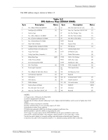
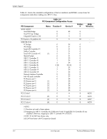
Processor/Memory Subsystem The SPD address map is shown in Table 3-2. Byte 0 1 2 3 4 5 6, 7 8 9 10 11 12 13 14 15 16 17 18 19 20 21 22 23 24 Table 3-2 SPD Address Map (SDRAM DIMM) Description Notes Byte Description No. of Bytes Written Into EEPROM Total Bytes (#) In EEPROM Memory Type No. of Row Addresses On DIMM No. of Column Addresses On DIMM No. of Module Banks On DIMM Data Width of Module Voltage Interface Standard of DIMM Cycletime @ Max CAS Latency (CL) Access From Clock Config. Type (Parity, Nonparity...) Refresh Rate/Type Width, Primary DRAM Error Checking Data Width Min. Clock Delay Burst Lengths Supported No. of Banks For Each Mem. Device CAS Latencies Supported CS# Latency Write Latency DIMM Attributes Memory Device Attributes Min. CLK Cycle Time at CL X-1 Max. Acc. Time From CLK @ CL X-1 [1] [2] [3] [4] [4] [4][5] [6] [4] [4] [4] [4] [7] [7] 25 26 27 28 29 30-31 32-61 62 63 64-71 72 73-90 91-92 93-94 95-98 99125 126 127 128 - 131 132 133 - 145 146 147 148 Min. CLK Cycle Time at CL X-2 Max. Acc. Time From CLK @ CL X-2 Min. Row Prechge. Time Min. Row Active to Delay Min. RAS to CAS Delay Reserved Superset Data SPD Revision Checksum Bytes 0-62 JEP-106E ID Code DIMM OEM Location OEM's Part Number OEM's Rev. Code Manufacture Date OEM's Assembly S/N OEM Specific Data Intel frequency check Reserved Compaq header "CPQ1" Header checksum Unit serial number DIMM ID Checksum Reserved Notes [7] [7] [7] [7] [7] [7] [7] [8] [8] [8] [8] [8] [8] [8] [9] [9] [9][10] [9][11] [9] [9] NOTES: [1] Programmed as 128 bytes by the DIMM OEM [2] Must be programmed to 256 bytes. [3] High order bit defines redundant addressing: if set (1), highest order RAS# address must be re-sent as highest order CAS# address. [4] Refer to memory manufacturer's datasheet [5] MSb is Self Refresh flag. If set (1), assembly supports self refresh. [6] Back-to-back random column addresses. [7] Field format proposed to JEDEC but not defined as standard at publication time. [8] Field specified as optional by JEDEC but required by this system. [9] HP usage. This system requires that the DIMM EEPROM have this space available for reads/writes. [10] Serial # in ASCII format (MSB is 133). Intended as backup identifier in case vender data is invalid. Can also be used to indicate s/n mismatch and flag system adminstrator of possible system Tampering. [11]Contains the socket # of the module (first module is "1"). Intended as backup identifier (refer to note [10]). Technical Reference Guide www.hp.com 3-7
-
 1
1 -
2
-
3
-
4
-
5
-
6
-
7
-
8
-
9
-
10
-
11
-
12
-
13
-
14
-
15
-
16
-
17
-
18
-
19
-
20
-
21
-
22
-
23
-
24
-
25
-
26
-
27
-
28
-
29
-
30
-
31
-
32
-
33
-
34
-
35
-
36
-
37
-
38
-
39
-
40
-
41
-
42
-
43
-
44
-
45
-
 46
46 -
 47
47 -
 48
48 -
 49
49 -
 50
50 -
 51
51 -
 52
52 -
 53
53 -
 54
54 -
 55
55 -
 56
56 -
57
-
58
-
59
-
60
-
61
-
62
-
63
-
64
-
65
-
66
-
67
-
68
-
69
-
70
-
71
-
72
-
73
-
74
-
75
-
76
-
77
-
78
-
79
-
80
-
81
-
82
-
83
-
84
-
85
-
86
-
87
-
88
-
89
-
90
-
91
-
92
-
93
-
94
-
95
-
96
-
97
-
98
-
99
-
100
-
101
-
102
-
103
-
104
-
105
-
106
-
107
-
108
-
109
-
110
-
111
-
112
-
113
-
114
-
115
-
116
-
117
-
118
-
119
-
120
-
121
-
122
-
123
-
124
-
125
-
126
-
127
-
128
-
129
-
130
-
131
-
132
-
133
-
134
-
135
-
136
-
137
-
138
-
139
-
140
-
141
-
142
-
143
-
144
-
145
-
146
-
147
-
148
-
149
-
150
-
151
-
152
-
153
-
154
-
155
-
156
-
157
-
158
-
159
-
160
-
161
-
162
-
163
-
164
-
165
-
166
-
167
-
168
-
169
-
170
-
171
-
172
-
173
-
174
-
175
-
176
-
177
-
178
-
179
-
180
-
181
-
182
-
183
-
184
-
185
-
186
-
187
-
188
-
189
-
190
-
191
-
192
-
193
-
194
-
195
-
196
 |
 |