HP Dc7700 HP Compaq dx7300 and dc7700 Business PC Technical Reference Guide, 1 - Page 54
PCI 2.3 Bus Operation, I/O and Memory Cycles
 |
UPC - 882780715318
View all HP Dc7700 manuals
Add to My Manuals
Save this manual to your list of manuals |
Page 54 highlights
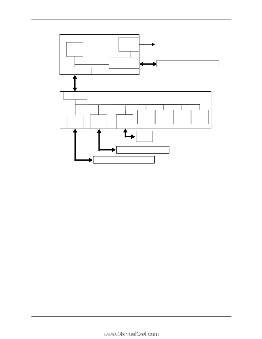
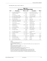
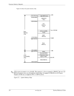
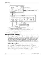
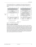
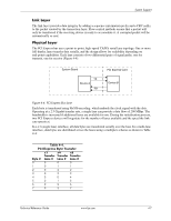
System Support Memory Cntlr Function Q965 GMCH PCI Bus 0 Host-DMI Bridge Integrated Graphics Controller Host-PCI Exp. Bridge RGB Monitor PCI Express x16 graphics slot [1] DMI Link DMI PCI 2.3 Bridge Function PCI Exp. Port 1 Function 82801 ICH8 PCI Bus 1 NIC. Function SATA USB I/F LPC HD Audio Cntlr Cntlr Bridge Cntlr Function Function Function Function NIC I/F PCI Express x1 slot PCI 2.3 slot(s) Notes: Only implemented functions are shown. [1] In USDT SFF, and ST form factors, accepts reverse-layout graphics cards. In MT and CMT form factors, accepts nomal layout graphics card. Figure 4-1. PCI Bus Devices and Functions 4.2.1 PCI 2.3 Bus Operation The PCI 2.3 bus consists of a 32-bit path (AD31-00 lines) that uses a multiplexed scheme for handling both address and data transfers. A bus transaction consists of an address cycle and one or more data cycles, with each cycle requiring a clock (PCICLK) cycle. High performance is realized during burst modes in which a transaction with contiguous memory locations requires that only one address cycle be conducted and subsequent data cycles are completed using auto-incremented addressing. Four types of address cycles can take place on the PCI bus; I/O, memory, configuration, and special. Address decoding is distributed (left up to each device on the PCI bus). I/O and Memory Cycles For I/O and memory cycles, a standard 32-bit address decode (AD31..0) for byte-level addressing is handled by the appropriate PCI device. For memory addressing, PCI devices decode the AD31..2 lines for dword-level addressing and check the AD1,0 lines for burst (linear-incrementing) mode. In burst mode, subsequent data phases are conducted a dword at a time with addressing assumed to increment accordingly (four bytes at a time). 4-2 www.hp.com Technical Reference Guide
-
 1
1 -
2
-
3
-
4
-
5
-
6
-
7
-
8
-
9
-
10
-
11
-
12
-
13
-
14
-
15
-
16
-
17
-
18
-
19
-
20
-
21
-
22
-
23
-
24
-
25
-
26
-
27
-
28
-
29
-
30
-
31
-
32
-
33
-
34
-
35
-
36
-
37
-
38
-
39
-
40
-
41
-
42
-
43
-
44
-
45
-
46
-
47
-
48
-
 49
49 -
 50
50 -
 51
51 -
 52
52 -
 53
53 -
 54
54 -
 55
55 -
 56
56 -
 57
57 -
 58
58 -
 59
59 -
60
-
61
-
62
-
63
-
64
-
65
-
66
-
67
-
68
-
69
-
70
-
71
-
72
-
73
-
74
-
75
-
76
-
77
-
78
-
79
-
80
-
81
-
82
-
83
-
84
-
85
-
86
-
87
-
88
-
89
-
90
-
91
-
92
-
93
-
94
-
95
-
96
-
97
-
98
-
99
-
100
-
101
-
102
-
103
-
104
-
105
-
106
-
107
-
108
-
109
-
110
-
111
-
112
-
113
-
114
-
115
-
116
-
117
-
118
-
119
-
120
-
121
-
122
-
123
-
124
-
125
-
126
-
127
-
128
-
129
-
130
-
131
-
132
-
133
-
134
-
135
-
136
-
137
-
138
-
139
-
140
-
141
-
142
-
143
-
144
-
145
-
146
-
147
-
148
-
149
-
150
-
151
-
152
-
153
-
154
-
155
-
156
-
157
-
158
-
159
-
160
-
161
-
162
-
163
-
164
-
165
-
166
-
167
-
168
-
169
-
170
-
171
-
172
-
173
-
174
-
175
-
176
-
177
-
178
-
179
-
180
-
181
-
182
-
183
-
184
-
185
-
186
-
187
-
188
-
189
-
190
-
191
-
192
-
193
-
194
-
195
-
196
 |
 |