HP Dc7700 HP Compaq dx7300 and dc7700 Business PC Technical Reference Guide, 1 - Page 59
Link Layer, Physical Layer, Table 4-4., PCI Express Byte Transfer
 |
UPC - 882780715318
View all HP Dc7700 manuals
Add to My Manuals
Save this manual to your list of manuals |
Page 59 highlights
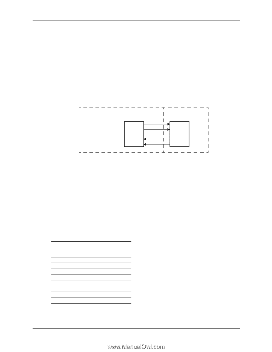
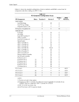
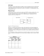
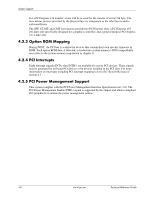
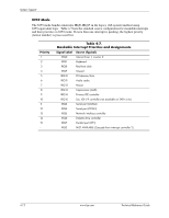
System Support Link Layer The link layer provides data integrity by adding a sequence information prefix and a CRC suffix to the packet created by the transaction layer. Flow-control methods ensure that a packet will only be transferred if the receiving device is ready to accomodate it. A corrupted packet will be automatically re-sent. Physical Layer The PCI Express bus uses a point-to-point, high-speed TX/RX serial lane topology. One or more full-duplex lanes transfer data serially, and the design allows for scalability depending on end-point capabilities. Each lane consists of two differential pairs of signal paths; one for transmit, one for receive (Figure 4-4). System Board TX Device A RX PCI Express Card Device B Figure 4-4. PCI Express Bus Lane Each byte is transferred using 8b/10b encoding. which embeds the clock signal with the data. Operating at a 2.5 Gigabit transfer rate, a single lane can provide a data flow of 200 MBps. The bandwidth is increased if additional lanes are available for use. During the initialization process, two PCI Express devices will negotiate for the number of lanes available and the speed the link can operate at. In a x1 (single lane) interface, all data bytes are transferred serially over the lane. In a multi-lane interface, data bytes are distributed across the lanes using a multiplex scheme as shown in Table 4-4: Table 4-4. PCI Express Byte Transfer Byte # x1 x4 x8 Transfer Transfer Transfer Lane # Lane # Lane # 0 0 0 0 1 0 1 1 2 0 2 2 3 0 3 3 4 0 0 4 5 0 1 5 6 0 2 6 7 0 3 7 Technical Reference Guide www.hp.com 4-7
-
 1
1 -
2
-
3
-
4
-
5
-
6
-
7
-
8
-
9
-
10
-
11
-
12
-
13
-
14
-
15
-
16
-
17
-
18
-
19
-
20
-
21
-
22
-
23
-
24
-
25
-
26
-
27
-
28
-
29
-
30
-
31
-
32
-
33
-
34
-
35
-
36
-
37
-
38
-
39
-
40
-
41
-
42
-
43
-
44
-
45
-
46
-
47
-
48
-
49
-
50
-
51
-
52
-
53
-
 54
54 -
 55
55 -
 56
56 -
 57
57 -
 58
58 -
 59
59 -
 60
60 -
 61
61 -
 62
62 -
 63
63 -
 64
64 -
65
-
66
-
67
-
68
-
69
-
70
-
71
-
72
-
73
-
74
-
75
-
76
-
77
-
78
-
79
-
80
-
81
-
82
-
83
-
84
-
85
-
86
-
87
-
88
-
89
-
90
-
91
-
92
-
93
-
94
-
95
-
96
-
97
-
98
-
99
-
100
-
101
-
102
-
103
-
104
-
105
-
106
-
107
-
108
-
109
-
110
-
111
-
112
-
113
-
114
-
115
-
116
-
117
-
118
-
119
-
120
-
121
-
122
-
123
-
124
-
125
-
126
-
127
-
128
-
129
-
130
-
131
-
132
-
133
-
134
-
135
-
136
-
137
-
138
-
139
-
140
-
141
-
142
-
143
-
144
-
145
-
146
-
147
-
148
-
149
-
150
-
151
-
152
-
153
-
154
-
155
-
156
-
157
-
158
-
159
-
160
-
161
-
162
-
163
-
164
-
165
-
166
-
167
-
168
-
169
-
170
-
171
-
172
-
173
-
174
-
175
-
176
-
177
-
178
-
179
-
180
-
181
-
182
-
183
-
184
-
185
-
186
-
187
-
188
-
189
-
190
-
191
-
192
-
193
-
194
-
195
-
196
 |
 |