Epson LQ 1050 Technical Manual - Page 188
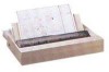
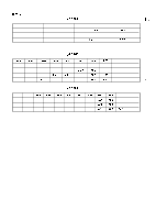
CPU KPD781OHG, A-1. KPD7810/7811 Pin Diagram
 |
View all Epson LQ 1050 manuals
Add to My Manuals
Save this manual to your list of manuals |
Page 188 highlights
REV.-A A.1.l CPU KPD781OHG The wPD78 10/781 1 is an 8-bit CPU and includes two 8 bit timer counters, an 8-bit A/D converter, 256 bytes of RAM, and a serial interface. A system can be easily constructed using this IC. The main features of this IC are as follows. q 256 bytes built-in RAM (addresses FFOOH-FFFFH) q 4096 bytes maks ROM (addresses O-FFOOH) for the 7811 CPU q Direct addressing of up to 64K bytes . 8-bit A/D converter q 158 instructions q 0.8 KS instruction cycle (15 MHz) q 16-bit event counter q Two 8-bit timer counters q 3 external and 8 internal interrupts; 6 priority levels and 6 interrupt addresses. q General purpose serial interface (asynchronous, synchronous, and 1/0 modes) q 1/0 line (781 1 :40-bit 1/0 port; 78 10:24-bit edge detection, 4 inputs) L q Zero corss detection q Standby function q Built-in clock pulse circuit q NMOS Figures A-1 and A-2 illustrate the 78 10/781 1 HG microprocessor, and Tables A-3 through A-6 describe its functions. PAO PA 1 PA2 PA3 PA4 PAS PA6 PA7 PBO Pal P82 PB3 PB4 PBS PB6 P87 Pco Pcl PC2 PC3 P124 Pcs PC6 PC7 ml INT 1 MODE 1 RESET MOOEO x2 xl v Ss 5 ~6 - 7 - 8 ~9 - 10 - 11 - 12 - 13 - 14 - 15 - 16 - 17 ~ 18 ~ -H - 21 - 22 - 23 - - :: ~ 26 :; % 29 36 30 31 X u 32 3 3 vu Voo PD7 P06 P05 P04 PD3 P02 Pol Poo PF7 PF6 PF5 PF4 PF3 PF2 PF 1 PFO ALE G m AVCC VAREF AN7 AN6 AN5 AN4 AN3 AN2 AN] ANO AV ss Figure A-1. KPD7810/7811 Pin Diagram A-2
-
 1
1 -
2
-
3
-
4
-
5
-
6
-
7
-
8
-
9
-
10
-
11
-
12
-
13
-
14
-
15
-
16
-
17
-
18
-
19
-
20
-
21
-
22
-
23
-
24
-
25
-
26
-
27
-
28
-
29
-
30
-
31
-
32
-
33
-
34
-
35
-
36
-
37
-
38
-
39
-
40
-
41
-
42
-
43
-
44
-
45
-
46
-
47
-
48
-
49
-
50
-
51
-
52
-
53
-
54
-
55
-
56
-
57
-
58
-
59
-
60
-
61
-
62
-
63
-
64
-
65
-
66
-
67
-
68
-
69
-
70
-
71
-
72
-
73
-
74
-
75
-
76
-
77
-
78
-
79
-
80
-
81
-
82
-
83
-
84
-
85
-
86
-
87
-
88
-
89
-
90
-
91
-
92
-
93
-
94
-
95
-
96
-
97
-
98
-
99
-
100
-
101
-
102
-
103
-
104
-
105
-
106
-
107
-
108
-
109
-
110
-
111
-
112
-
113
-
114
-
115
-
116
-
117
-
118
-
119
-
120
-
121
-
122
-
123
-
124
-
125
-
126
-
127
-
128
-
129
-
130
-
131
-
132
-
133
-
134
-
135
-
136
-
137
-
138
-
139
-
140
-
141
-
142
-
143
-
144
-
145
-
146
-
147
-
148
-
149
-
150
-
151
-
152
-
153
-
154
-
155
-
156
-
157
-
158
-
159
-
160
-
161
-
162
-
163
-
164
-
165
-
166
-
167
-
168
-
169
-
170
-
171
-
172
-
173
-
174
-
175
-
176
-
177
-
178
-
179
-
180
-
181
-
182
-
 183
183 -
 184
184 -
 185
185 -
 186
186 -
 187
187 -
 188
188 -
 189
189 -
 190
190 -
 191
191 -
 192
192 -
 193
193 -
194
-
195
-
196
-
197
-
198
-
199
-
200
-
201
-
202
-
203
-
204
-
205
-
206
-
207
-
208
-
209
-
210
-
211
-
212
-
213
-
214
-
215
-
216
-
217
-
218
-
219
-
220
-
221
-
222
-
223
-
224
-
225
 |
 |