Epson LQ 1050 Technical Manual - Page 192
A-3. OP Code Fetch Timing
 |
View all Epson LQ 1050 manuals
Add to My Manuals
Save this manual to your list of manuals |
Page 192 highlights
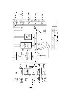
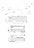
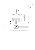
REV.-A q CPU Timing "['''"" Refer to Figures A-3 through A-5 for CPU timing diagrams. Three oscillations define one state. The OP code fetch requires four states; during TI to T3, program memory is read; instructions are interpreted during T4. Address bus lines 15-8 are output from T1 to T4. Address but lines 7-O (PD7-0) are used in the multiplex mode; the address is latched during T1 at the ALE signal. Since the memory addressed is enabled after disengaging the driver (AD7-0), ~ is output from T1 -T3, fetched at T3, and processed internally at T4. The ALE and RD signals are executed from T1-T3; the OP code fetch for these two signals is performed at T4. The WR signal is output from the middle of T 1 to the beginning of T3. The address and ALE timing is the same as that for memory read; however following address output AD7-O (PD7-0) are not disabled, and write data is output at AD7-O at the beginning of T1 and the end of T3. NOTE: When PD7-O are set to the multiplexed address/data-bus (AD7-0) to the address bus (AB7-0), the ~ and WR signals in the machine cycle are HIGH when memory is not being accessed. CLOCK ALE AB15 -8 (PF7 -O) AD7 -o (PD7 -O) Y ADDRESS x A D D R E S S }- - - - < OP CODE / x >---c Figure A-3. OP Code Fetch Timing T1 T2 T3 CLOCK ~ AB15 -8 (PF7 -0) AD7 -o (PD7 -O) x ADDRESS x x A D D R E S S }- --< READ DATA >--- c Figure A-4. Memory Read Timing CLOCK AB15 -8 (PF7 -0) AD7 -0 (PD7 -0) x ADDRESS x x x ADDRESS WRITE DATA Figure A-5. Memory Write Timing A-6
-
 1
1 -
2
-
3
-
4
-
5
-
6
-
7
-
8
-
9
-
10
-
11
-
12
-
13
-
14
-
15
-
16
-
17
-
18
-
19
-
20
-
21
-
22
-
23
-
24
-
25
-
26
-
27
-
28
-
29
-
30
-
31
-
32
-
33
-
34
-
35
-
36
-
37
-
38
-
39
-
40
-
41
-
42
-
43
-
44
-
45
-
46
-
47
-
48
-
49
-
50
-
51
-
52
-
53
-
54
-
55
-
56
-
57
-
58
-
59
-
60
-
61
-
62
-
63
-
64
-
65
-
66
-
67
-
68
-
69
-
70
-
71
-
72
-
73
-
74
-
75
-
76
-
77
-
78
-
79
-
80
-
81
-
82
-
83
-
84
-
85
-
86
-
87
-
88
-
89
-
90
-
91
-
92
-
93
-
94
-
95
-
96
-
97
-
98
-
99
-
100
-
101
-
102
-
103
-
104
-
105
-
106
-
107
-
108
-
109
-
110
-
111
-
112
-
113
-
114
-
115
-
116
-
117
-
118
-
119
-
120
-
121
-
122
-
123
-
124
-
125
-
126
-
127
-
128
-
129
-
130
-
131
-
132
-
133
-
134
-
135
-
136
-
137
-
138
-
139
-
140
-
141
-
142
-
143
-
144
-
145
-
146
-
147
-
148
-
149
-
150
-
151
-
152
-
153
-
154
-
155
-
156
-
157
-
158
-
159
-
160
-
161
-
162
-
163
-
164
-
165
-
166
-
167
-
168
-
169
-
170
-
171
-
172
-
173
-
174
-
175
-
176
-
177
-
178
-
179
-
180
-
181
-
182
-
183
-
184
-
185
-
186
-
 187
187 -
 188
188 -
 189
189 -
 190
190 -
 191
191 -
 192
192 -
 193
193 -
 194
194 -
 195
195 -
 196
196 -
 197
197 -
198
-
199
-
200
-
201
-
202
-
203
-
204
-
205
-
206
-
207
-
208
-
209
-
210
-
211
-
212
-
213
-
214
-
215
-
216
-
217
-
218
-
219
-
220
-
221
-
222
-
223
-
224
-
225
 |
 |
