Epson LQ 1050 Technical Manual - Page 71
A and 3A.
 |
View all Epson LQ 1050 manuals
Add to My Manuals
Save this manual to your list of manuals |
Page 71 highlights
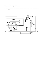
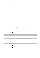
2.3.3 Main IC Functions This section describes the functions of the main ICS in the PEGX board control circuit. REV.-A 2.3.3.1 CPU Functions The printer employs the pPD78 10HG CPU. The CPU processes data using a 3.685 MHz clock which is 1/4 of the external clock (14.74 MHz.) The CPU is reset when the reset signal (pin 28: LOW) is input, and executes the external program (4A, PROM) from address O. The CPU controls all of the printer operations either directly or indirectly. The external memory area is expanded to 64K bytes so that the CPU can control the internal RAM, external ROM (4A: program and character generator), external SRAMS (5A and 6A), and the E05A16G and E05A15A gate arrays (7A and 3A). NOTE: Refer to Section 2.3.1.3 for memory mapping. This CPU includes an 8-bit analog-to-digital converter, timer-event counter, and serial interface. These functions can be set in units of bits using the mode register for each port, and are used with general 1/0 ports (excluding the analog-to-digital converter.) Table 2-3 shows the port assignments. (Refer to the Appendix for details on the CPU.) Pin No. 1 I 6 7 8 9 I 16 17 18 19 20 21 22 23 24 25 Table 2-3. Pin Function of CPU Signal Name PAO I PA5 PA6 PA7 PBO I PB7 Pco Pcl PC2 PC3 PC4 PC5 PC6 PC7 NM 1 Direction - Not used. Function IN AUTO FEED XT signal/DIP switch 2-4 IN SLCT IN signal/Jumper J 1 IN DIP switch 1-1 to 1-8 OUT TXD data output IN RXD data input - Not used IN ON-LINE switch interrupt input - Not used IN P/S (Parallel/Serial) data transfer selection signal input OUT PWD signal output OUT Paper feed motor driving control output - Not used 2-27
-
 1
1 -
2
-
3
-
4
-
5
-
6
-
7
-
8
-
9
-
10
-
11
-
12
-
13
-
14
-
15
-
16
-
17
-
18
-
19
-
20
-
21
-
22
-
23
-
24
-
25
-
26
-
27
-
28
-
29
-
30
-
31
-
32
-
33
-
34
-
35
-
36
-
37
-
38
-
39
-
40
-
41
-
42
-
43
-
44
-
45
-
46
-
47
-
48
-
49
-
50
-
51
-
52
-
53
-
54
-
55
-
56
-
57
-
58
-
59
-
60
-
61
-
62
-
63
-
64
-
65
-
 66
66 -
 67
67 -
 68
68 -
 69
69 -
 70
70 -
 71
71 -
 72
72 -
 73
73 -
 74
74 -
 75
75 -
 76
76 -
77
-
78
-
79
-
80
-
81
-
82
-
83
-
84
-
85
-
86
-
87
-
88
-
89
-
90
-
91
-
92
-
93
-
94
-
95
-
96
-
97
-
98
-
99
-
100
-
101
-
102
-
103
-
104
-
105
-
106
-
107
-
108
-
109
-
110
-
111
-
112
-
113
-
114
-
115
-
116
-
117
-
118
-
119
-
120
-
121
-
122
-
123
-
124
-
125
-
126
-
127
-
128
-
129
-
130
-
131
-
132
-
133
-
134
-
135
-
136
-
137
-
138
-
139
-
140
-
141
-
142
-
143
-
144
-
145
-
146
-
147
-
148
-
149
-
150
-
151
-
152
-
153
-
154
-
155
-
156
-
157
-
158
-
159
-
160
-
161
-
162
-
163
-
164
-
165
-
166
-
167
-
168
-
169
-
170
-
171
-
172
-
173
-
174
-
175
-
176
-
177
-
178
-
179
-
180
-
181
-
182
-
183
-
184
-
185
-
186
-
187
-
188
-
189
-
190
-
191
-
192
-
193
-
194
-
195
-
196
-
197
-
198
-
199
-
200
-
201
-
202
-
203
-
204
-
205
-
206
-
207
-
208
-
209
-
210
-
211
-
212
-
213
-
214
-
215
-
216
-
217
-
218
-
219
-
220
-
221
-
222
-
223
-
224
-
225
 |
 |
