Epson LQ 1050 Technical Manual - Page 191
LPD781, Sginal
 |
View all Epson LQ 1050 manuals
Add to My Manuals
Save this manual to your list of manuals |
Page 191 highlights
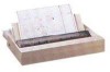
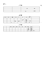
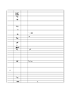
REV.-A Table A-6. 1.LPD781 0/781 1 Port Functions Pin Sginal Direction Descriptions 1-8 PAO-7 In/Out Port A: Eight-bit l/O with output latch. l/O possible by mode A (MA) register. Output HIGH. 9-16 17-24 25 26 27, 29 PBO-7 PCO-7 NMI INT 1 MODE 1,0 In/Out In/Out In In In/Out Port B: Eight-bit 1/0 with output latch. l/O possible by mode B (MB) register. Output HIGH. Port C: Eight-bit 1/0 with output latch. Port/Control mode can be set by mode control C (MCC) register. Output HIGH Non-maskable interrupt of the edge trigger (trailing edge). Maskable interrupt input of the edge trigger (leading edge). Also used as the AC input zero cross detecting terminal. 7811 :O=LOW and 1 =HIGH 7810 modes set in accordance with external memory (see Table A-2) 28 30, 31 32 33 34-41 42 43 44 45 46 47-54 55-62 63 64 RESET X2,X1 Vss AVSS ANO-7 VAref AVCC RD WR ALE PFO-7 PDO-7 VDD Vcc In - - - In In - out out out LOW reset Crytal connection for built-in clock pulse. When clock pulses are supplied externally, input must be to X 1. Supply voltage, Vss, OV Analong Vss Eight analog inputs of the A/D converter. AN7-4 can be used as the input terminals to the detect the leading edge and to set the test flag upon detection of the trailing edge. Reference voltage Analog Vcc Read strobe. LOW at the read machine cycle and at reset, HIGH at other times. Write strobe. LOW during the write machine cycle and at reset, HIGH at other times. Address latch enable. Latches the lower 8 address bits to access external memory. Port F 78: 1 1: Port bit-by-bit 1/0 possible by mode F register. In extension mode gradual address output assignment is possible in accordance with the size of external memory. See Table A-3. 78 10: By setting modes O and 1, assignment to the address bus (AB 15-8) can be made in accordance with the size of the external memory. The remaining terminals can be used as l/O ports. See Table A-4. Port D 781 1: Port bit-by-bit 1/0 possible. In extension mode, PD7-O act as the multiplexed address/data but (AD7-0). 78 10: Multiplexed address/data bus to access external memory. Supply voltage, VDD +5v Supply voltage, Vcc +5v NOTE: "Direction" refers to the direction of signal flow as viewed from the CPU. A-5
-
 1
1 -
2
-
3
-
4
-
5
-
6
-
7
-
8
-
9
-
10
-
11
-
12
-
13
-
14
-
15
-
16
-
17
-
18
-
19
-
20
-
21
-
22
-
23
-
24
-
25
-
26
-
27
-
28
-
29
-
30
-
31
-
32
-
33
-
34
-
35
-
36
-
37
-
38
-
39
-
40
-
41
-
42
-
43
-
44
-
45
-
46
-
47
-
48
-
49
-
50
-
51
-
52
-
53
-
54
-
55
-
56
-
57
-
58
-
59
-
60
-
61
-
62
-
63
-
64
-
65
-
66
-
67
-
68
-
69
-
70
-
71
-
72
-
73
-
74
-
75
-
76
-
77
-
78
-
79
-
80
-
81
-
82
-
83
-
84
-
85
-
86
-
87
-
88
-
89
-
90
-
91
-
92
-
93
-
94
-
95
-
96
-
97
-
98
-
99
-
100
-
101
-
102
-
103
-
104
-
105
-
106
-
107
-
108
-
109
-
110
-
111
-
112
-
113
-
114
-
115
-
116
-
117
-
118
-
119
-
120
-
121
-
122
-
123
-
124
-
125
-
126
-
127
-
128
-
129
-
130
-
131
-
132
-
133
-
134
-
135
-
136
-
137
-
138
-
139
-
140
-
141
-
142
-
143
-
144
-
145
-
146
-
147
-
148
-
149
-
150
-
151
-
152
-
153
-
154
-
155
-
156
-
157
-
158
-
159
-
160
-
161
-
162
-
163
-
164
-
165
-
166
-
167
-
168
-
169
-
170
-
171
-
172
-
173
-
174
-
175
-
176
-
177
-
178
-
179
-
180
-
181
-
182
-
183
-
184
-
185
-
 186
186 -
 187
187 -
 188
188 -
 189
189 -
 190
190 -
 191
191 -
 192
192 -
 193
193 -
 194
194 -
 195
195 -
 196
196 -
197
-
198
-
199
-
200
-
201
-
202
-
203
-
204
-
205
-
206
-
207
-
208
-
209
-
210
-
211
-
212
-
213
-
214
-
215
-
216
-
217
-
218
-
219
-
220
-
221
-
222
-
223
-
224
-
225
 |
 |