Epson LQ 1050 Technical Manual - Page 23
Auto Feed Xt
 |
View all Epson LQ 1050 manuals
Add to My Manuals
Save this manual to your list of manuals |
Page 23 highlights
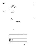
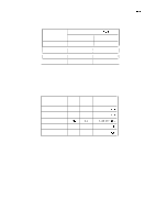
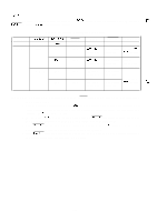
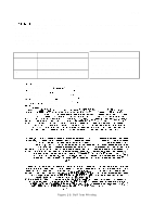
REV.-A ~,. Table 1-17 shows the connector pin assignments and signal functions of the 8-bit parallel interface. < . ,' Table 1-17. Connector Pin Assignments and Signal Function Pin No. 1 2 3 4 5 6 7 8 9 10 11 12 13 14 15 16 17 18 19 - 3 0 31 32 Signal Name STRORE DATA 1 DATA 2 DATA 3 DATA 4 DATA 5 DATA 6 DATA 7 DATA 8 ACKNLG BUSY PE AUTO FEED XT NC Ov CHASSIS GND NC GND INIT ERROR Return Pin No. DIR Functional Description 19 In Strobe pulse to read the input data. Pulse width must be more than 0.5#s. Input data is latched after falling edge of this signal. 20 In These signals represent information of the 1st to 8th 21 In bits of parallel data, respectively. Each signal is at 22 In "HIGH" level when data is logical "1" and "LOW" when 23 In logical "O". 24 In 25 In 26 In 27 In 28 out This pulse indicates data has been received and the printer is ready to accept more data. Pulse width is approximately 12#s. 29 out A "HIGH" signal indicates that the printer cannot receive data. The signal becomes "HIGH" in the follow- ing cases: 1. During data entry 2. During printing operation 3. In off-line status 4. During printer error status 30 out A "HIGH" signal indicates that the printer is out of paper. Pulled up to +5V through 3.3 K ohms resistor. In With this signal at "LOW"' level, the paper is automatically fed one line after printing. (The signal level can be fixed to "LOW"' with DIP SW 2-4.) Not used. Logic GND level. Printer chassis GND. In the printer, the chassis GND and the logic GND are isolated from each other. Not used. TWISTED-PAIR RETURN signal GND level. In When the level of this signal become "LOW", the printer controller is reset to its initial state and the print buffer is cleared. This signal is normally at "HIGH" level, and its pulse width must be more than 50 @ at the receiving terminal. out The level of this signal becomes "LOW" when the printer is in 1. Paper-out status 2. Off-line status 3. Error status 1-14
-
 1
1 -
2
-
3
-
4
-
5
-
6
-
7
-
8
-
9
-
10
-
11
-
12
-
13
-
14
-
15
-
16
-
17
-
 18
18 -
 19
19 -
 20
20 -
 21
21 -
 22
22 -
 23
23 -
 24
24 -
 25
25 -
 26
26 -
 27
27 -
 28
28 -
29
-
30
-
31
-
32
-
33
-
34
-
35
-
36
-
37
-
38
-
39
-
40
-
41
-
42
-
43
-
44
-
45
-
46
-
47
-
48
-
49
-
50
-
51
-
52
-
53
-
54
-
55
-
56
-
57
-
58
-
59
-
60
-
61
-
62
-
63
-
64
-
65
-
66
-
67
-
68
-
69
-
70
-
71
-
72
-
73
-
74
-
75
-
76
-
77
-
78
-
79
-
80
-
81
-
82
-
83
-
84
-
85
-
86
-
87
-
88
-
89
-
90
-
91
-
92
-
93
-
94
-
95
-
96
-
97
-
98
-
99
-
100
-
101
-
102
-
103
-
104
-
105
-
106
-
107
-
108
-
109
-
110
-
111
-
112
-
113
-
114
-
115
-
116
-
117
-
118
-
119
-
120
-
121
-
122
-
123
-
124
-
125
-
126
-
127
-
128
-
129
-
130
-
131
-
132
-
133
-
134
-
135
-
136
-
137
-
138
-
139
-
140
-
141
-
142
-
143
-
144
-
145
-
146
-
147
-
148
-
149
-
150
-
151
-
152
-
153
-
154
-
155
-
156
-
157
-
158
-
159
-
160
-
161
-
162
-
163
-
164
-
165
-
166
-
167
-
168
-
169
-
170
-
171
-
172
-
173
-
174
-
175
-
176
-
177
-
178
-
179
-
180
-
181
-
182
-
183
-
184
-
185
-
186
-
187
-
188
-
189
-
190
-
191
-
192
-
193
-
194
-
195
-
196
-
197
-
198
-
199
-
200
-
201
-
202
-
203
-
204
-
205
-
206
-
207
-
208
-
209
-
210
-
211
-
212
-
213
-
214
-
215
-
216
-
217
-
218
-
219
-
220
-
221
-
222
-
223
-
224
-
225
 |
 |
