Epson LQ 1050 Technical Manual - Page 66
be-pin
 |
View all Epson LQ 1050 manuals
Add to My Manuals
Save this manual to your list of manuals |
Page 66 highlights
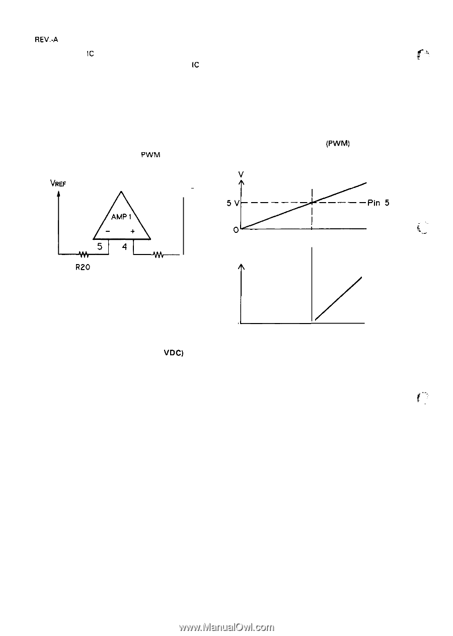
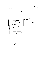
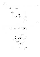
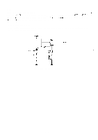
REV.-A AMP 1 in the IC is an error amplifier used to monitor the output voltage. Figure 20 shows the constant-voltage control circuit. Pin 1 of the IC provides a 5 V reference output (Vref), which is applied to the negative terminal of AMP 1. The error amplifier adjusts its output according to the voltages applied to the positive and negative input terminals. This has the effect of maintaining the voltage at the terminal at 5V. Figure 2-21 shows the output from AMP 1. When the voltage at pin 4 becomes higher than that at pin 5 (over voltage), AMP 1 outputs current modulated by pulse-width modulation (PWM) to reduce the output voltage of the circuit. PWM is described below. VREF R20 3. 3K OUTPUT Voltage - R 14 3. 3K Figure 2-20. Constant-Voltage Control (+5 VDC) v Pin 4 'r I 'be-pin' " Under Voltage Over Voltage ( Normal v Voltage ) L AMP 1 OUT PUT / o Figure 2-21. AMP 1 Output R 108 and C35 compensate for phase lag in the error amplifier to prevent abnormal oscillation. 2-22
-
 1
1 -
2
-
3
-
4
-
5
-
6
-
7
-
8
-
9
-
10
-
11
-
12
-
13
-
14
-
15
-
16
-
17
-
18
-
19
-
20
-
21
-
22
-
23
-
24
-
25
-
26
-
27
-
28
-
29
-
30
-
31
-
32
-
33
-
34
-
35
-
36
-
37
-
38
-
39
-
40
-
41
-
42
-
43
-
44
-
45
-
46
-
47
-
48
-
49
-
50
-
51
-
52
-
53
-
54
-
55
-
56
-
57
-
58
-
59
-
60
-
 61
61 -
 62
62 -
 63
63 -
 64
64 -
 65
65 -
 66
66 -
 67
67 -
 68
68 -
 69
69 -
 70
70 -
 71
71 -
72
-
73
-
74
-
75
-
76
-
77
-
78
-
79
-
80
-
81
-
82
-
83
-
84
-
85
-
86
-
87
-
88
-
89
-
90
-
91
-
92
-
93
-
94
-
95
-
96
-
97
-
98
-
99
-
100
-
101
-
102
-
103
-
104
-
105
-
106
-
107
-
108
-
109
-
110
-
111
-
112
-
113
-
114
-
115
-
116
-
117
-
118
-
119
-
120
-
121
-
122
-
123
-
124
-
125
-
126
-
127
-
128
-
129
-
130
-
131
-
132
-
133
-
134
-
135
-
136
-
137
-
138
-
139
-
140
-
141
-
142
-
143
-
144
-
145
-
146
-
147
-
148
-
149
-
150
-
151
-
152
-
153
-
154
-
155
-
156
-
157
-
158
-
159
-
160
-
161
-
162
-
163
-
164
-
165
-
166
-
167
-
168
-
169
-
170
-
171
-
172
-
173
-
174
-
175
-
176
-
177
-
178
-
179
-
180
-
181
-
182
-
183
-
184
-
185
-
186
-
187
-
188
-
189
-
190
-
191
-
192
-
193
-
194
-
195
-
196
-
197
-
198
-
199
-
200
-
201
-
202
-
203
-
204
-
205
-
206
-
207
-
208
-
209
-
210
-
211
-
212
-
213
-
214
-
215
-
216
-
217
-
218
-
219
-
220
-
221
-
222
-
223
-
224
-
225
 |
 |