AMD AMD-K6-2/500AFX Data Sheet - Page 28
Internal Architecture, AMD-K6, 2 Processor Data Sheet, EAX, EBX, ECX, EDX, EBP, ESP, ESI
 |
View all AMD AMD-K6-2/500AFX manuals
Add to My Manuals
Save this manual to your list of manuals |
Page 28 highlights
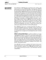
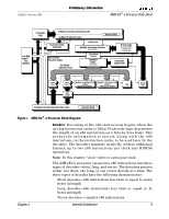
AMD-K6®-2 Processor Data Sheet Preliminary Information 21850J/0-February 2000 Short and long decodes are processed completely within the decoders. Vector decodes are started by the decoders and then completed by fetched sequences from an on-chip ROM. After decoding, the RISC86 operations are delivered to the scheduler for dispatching to the executions units. Scheduler/Instruction Control Unit. The centraliz ed scheduler or buffer is managed by the Instruction Control Unit (ICU). The ICU buffers and manages up to 24 RISC86 operations at a time. This equals from 6 to 12 x86 instructions. This buffer size (24) is perfectly matched to the processor's six-stage RISC86 pipeline and four RISC86-operations decode rate. The scheduler accepts as many as four RISC86 operations at a time from the decoders and retires up to four RISC86 operations per clock cycle. The ICU is capable of simultaneously issuing up to six RISC86 operations at a time to the execution units. This consists of the following types of operations: s Memory load operation s Memory store operation s Complex integer, MMX or 3DNow! register operation s Simple integer, MMX or 3DNow! register operation s Floating-point register operation s Branch condition evaluation Registers. When managing the 24 RISC86 operations, the ICU uses 69 physical registers contained within the RISC86 microarchitecture. 48 of the physical registers are located in a general register file and are grouped as 24 committed or architectural registers plus 24 rename registers. The 24 architectural registers consist of 16 scratch registers and 8 registers that correspond to the x86 general-purpose registers- EAX, EBX, ECX, EDX, EBP, ESP, ESI, and EDI. There is an analogous set of registers specifically for MMX and 3DNow! operations. There are 9 MMX/3DNow! committed or architectural registers plus 12 MMX/3DNow! rename registers. The 9 architectural registers consist of one scratch register and 8 registers that correspond to the MMX registers (mm0-mm7), as shown in Figure 17 on page 29. Branch Logic. The AMD-K6-2 processor is designed with highly sophisticated dynamic branch logic consisting of the following: s Branch history/Prediction table s Branch target cache s Return address stack 8 Internal Architecture Chapter 2
-
 1
1 -
2
-
3
-
4
-
5
-
6
-
7
-
8
-
9
-
10
-
11
-
12
-
13
-
14
-
15
-
16
-
17
-
18
-
19
-
20
-
21
-
22
-
 23
23 -
 24
24 -
 25
25 -
 26
26 -
 27
27 -
 28
28 -
 29
29 -
 30
30 -
 31
31 -
 32
32 -
 33
33 -
34
-
35
-
36
-
37
-
38
-
39
-
40
-
41
-
42
-
43
-
44
-
45
-
46
-
47
-
48
-
49
-
50
-
51
-
52
-
53
-
54
-
55
-
56
-
57
-
58
-
59
-
60
-
61
-
62
-
63
-
64
-
65
-
66
-
67
-
68
-
69
-
70
-
71
-
72
-
73
-
74
-
75
-
76
-
77
-
78
-
79
-
80
-
81
-
82
-
83
-
84
-
85
-
86
-
87
-
88
-
89
-
90
-
91
-
92
-
93
-
94
-
95
-
96
-
97
-
98
-
99
-
100
-
101
-
102
-
103
-
104
-
105
-
106
-
107
-
108
-
109
-
110
-
111
-
112
-
113
-
114
-
115
-
116
-
117
-
118
-
119
-
120
-
121
-
122
-
123
-
124
-
125
-
126
-
127
-
128
-
129
-
130
-
131
-
132
-
133
-
134
-
135
-
136
-
137
-
138
-
139
-
140
-
141
-
142
-
143
-
144
-
145
-
146
-
147
-
148
-
149
-
150
-
151
-
152
-
153
-
154
-
155
-
156
-
157
-
158
-
159
-
160
-
161
-
162
-
163
-
164
-
165
-
166
-
167
-
168
-
169
-
170
-
171
-
172
-
173
-
174
-
175
-
176
-
177
-
178
-
179
-
180
-
181
-
182
-
183
-
184
-
185
-
186
-
187
-
188
-
189
-
190
-
191
-
192
-
193
-
194
-
195
-
196
-
197
-
198
-
199
-
200
-
201
-
202
-
203
-
204
-
205
-
206
-
207
-
208
-
209
-
210
-
211
-
212
-
213
-
214
-
215
-
216
-
217
-
218
-
219
-
220
-
221
-
222
-
223
-
224
-
225
-
226
-
227
-
228
-
229
-
230
-
231
-
232
-
233
-
234
-
235
-
236
-
237
-
238
-
239
-
240
-
241
-
242
-
243
-
244
-
245
-
246
-
247
-
248
-
249
-
250
-
251
-
252
-
253
-
254
-
255
-
256
-
257
-
258
-
259
-
260
-
261
-
262
-
263
-
264
-
265
-
266
-
267
-
268
-
269
-
270
-
271
-
272
-
273
-
274
-
275
-
276
-
277
-
278
-
279
-
280
-
281
-
282
-
283
-
284
-
285
-
286
-
287
-
288
-
289
-
290
-
291
-
292
-
293
-
294
-
295
-
296
-
297
-
298
-
299
-
300
-
301
-
302
-
303
-
304
-
305
-
306
-
307
-
308
-
309
-
310
-
311
-
312
-
313
-
314
-
315
-
316
-
317
-
318
-
319
-
320
-
321
-
322
-
323
-
324
-
325
-
326
-
327
-
328
-
329
-
330
 |
 |
