AMD AMD-K6-2/500AFX Data Sheet - Page 29
Cache, Instruction Prefetch, and Predecode Bits, Cache, MESI Modified, Exclusive, Shared - 3d processor
 |
View all AMD AMD-K6-2/500AFX manuals
Add to My Manuals
Save this manual to your list of manuals |
Page 29 highlights
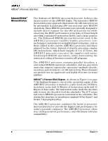
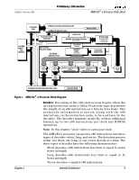
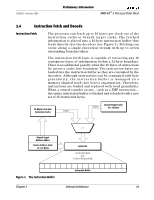
21850J/0-February 2000 Preliminary Information AMD-K6®-2 Processor Data Sheet 2.3 Cache The AMD-K6-2 processor implements a two-level branch prediction scheme based on an 8192-entry branch history table. The branch history table stores prediction information that is used for predicting conditional branches. Because the branch history table does not store predicted target addresses, special address ALUs calculate target addresses on-the-fly during instruction decode. The branch target cache augments predicted branch performance by avoiding a one clock cache-fetch penalty. This specialized target cache does this by supplying the first 16 bytes of target instructions to the decoders when branches are predicted. The return address stack is a unique device specifically designed for optimizing CALL and RETURN pairs. In summary, the AMD-K6-2 processor uses dynamic branch logic to minimize delays due to the branch instructions that are common in x86 software. 3DNow!™ Technology. AMD has taken a lead role in improving the multimedia and 3D capabilities of the x86 processor family with the introduction of 3DNow! technology, which uses a packed, single-precision, floating-point data format and Single Instruction Multiple Data (SIMD) operations based on the MMX technology model. Cache, Instruction Prefetch, and Predecode Bits The writeback level-one cache on the AMD-K6-2 processor is organized as a separate 32-Kbyte instruction cache and a 32-Kbyte data cache with two-way set associativity. The cache line size is 32 bytes and lines are prefetched from main memory using an efficient pipelined burst transaction. As the instruction cache is filled, each instruction byte is analyzed for instruction boundaries using predecoding logic. Predecoding annotates information (5 bits per byte) to each instruction byte that later enables the decoders to efficiently decode multiple instructions simultaneously. The processor cache design takes advantage of a sectored organization (see Figure 2 on page 10). Each sector consists of 64 bytes configured as two 32-byte cache lines. The two cache lines of a sector share a common tag but have separate pairs of MESI (Modified, Exclusive, Shared, Invalid) bits that track the state of each cache line. Chapter 2 Internal Architecture 9
-
 1
1 -
2
-
3
-
4
-
5
-
6
-
7
-
8
-
9
-
10
-
11
-
12
-
13
-
14
-
15
-
16
-
17
-
18
-
19
-
20
-
21
-
22
-
23
-
 24
24 -
 25
25 -
 26
26 -
 27
27 -
 28
28 -
 29
29 -
 30
30 -
 31
31 -
 32
32 -
 33
33 -
 34
34 -
35
-
36
-
37
-
38
-
39
-
40
-
41
-
42
-
43
-
44
-
45
-
46
-
47
-
48
-
49
-
50
-
51
-
52
-
53
-
54
-
55
-
56
-
57
-
58
-
59
-
60
-
61
-
62
-
63
-
64
-
65
-
66
-
67
-
68
-
69
-
70
-
71
-
72
-
73
-
74
-
75
-
76
-
77
-
78
-
79
-
80
-
81
-
82
-
83
-
84
-
85
-
86
-
87
-
88
-
89
-
90
-
91
-
92
-
93
-
94
-
95
-
96
-
97
-
98
-
99
-
100
-
101
-
102
-
103
-
104
-
105
-
106
-
107
-
108
-
109
-
110
-
111
-
112
-
113
-
114
-
115
-
116
-
117
-
118
-
119
-
120
-
121
-
122
-
123
-
124
-
125
-
126
-
127
-
128
-
129
-
130
-
131
-
132
-
133
-
134
-
135
-
136
-
137
-
138
-
139
-
140
-
141
-
142
-
143
-
144
-
145
-
146
-
147
-
148
-
149
-
150
-
151
-
152
-
153
-
154
-
155
-
156
-
157
-
158
-
159
-
160
-
161
-
162
-
163
-
164
-
165
-
166
-
167
-
168
-
169
-
170
-
171
-
172
-
173
-
174
-
175
-
176
-
177
-
178
-
179
-
180
-
181
-
182
-
183
-
184
-
185
-
186
-
187
-
188
-
189
-
190
-
191
-
192
-
193
-
194
-
195
-
196
-
197
-
198
-
199
-
200
-
201
-
202
-
203
-
204
-
205
-
206
-
207
-
208
-
209
-
210
-
211
-
212
-
213
-
214
-
215
-
216
-
217
-
218
-
219
-
220
-
221
-
222
-
223
-
224
-
225
-
226
-
227
-
228
-
229
-
230
-
231
-
232
-
233
-
234
-
235
-
236
-
237
-
238
-
239
-
240
-
241
-
242
-
243
-
244
-
245
-
246
-
247
-
248
-
249
-
250
-
251
-
252
-
253
-
254
-
255
-
256
-
257
-
258
-
259
-
260
-
261
-
262
-
263
-
264
-
265
-
266
-
267
-
268
-
269
-
270
-
271
-
272
-
273
-
274
-
275
-
276
-
277
-
278
-
279
-
280
-
281
-
282
-
283
-
284
-
285
-
286
-
287
-
288
-
289
-
290
-
291
-
292
-
293
-
294
-
295
-
296
-
297
-
298
-
299
-
300
-
301
-
302
-
303
-
304
-
305
-
306
-
307
-
308
-
309
-
310
-
311
-
312
-
313
-
314
-
315
-
316
-
317
-
318
-
319
-
320
-
321
-
322
-
323
-
324
-
325
-
326
-
327
-
328
-
329
-
330
 |
 |