HP Dc5700 HP Compaq dc5700 Business PC Service Reference Guide, 1st Edition - Page 208
SPI ROM and socket XU19 = socket, U19 = SPI ROM, System ROM and Socket Socket = XU15, ROM = U15
 |
UPC - 882780819535
View all HP Dc5700 manuals
Add to My Manuals
Save this manual to your list of manuals |
Page 208 highlights
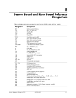
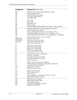
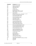
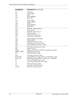
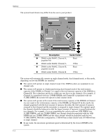
System Board and Riser Board Reference Designators Designator U6 U7 U10 U11 U12 U13 U14 U16 U17 U18 U19 U20 U21 U29 U30 U31 U32 U46 U50 U51 U52 U53 XBT XMM1 XMM2 - XMM5 XU1 XU2 XU15/U15 XU19/U19 Y1 Y2 Y3 Y4 Y5/H5 Component (Continued) Clock chip 64 bit Bridge LOM1 LOM1 EEPROM LOM1 PHY Audio Codec Audio amplifier LOM2 LOM2 EEPROM LOM2 PHY SPI ROM - SOIC-8 footprint Fan controller SPI ROM - SO16 footprint TMDS controller Parallel port diode array First serial port transceiver Second serial port transceiver VRM controller USB front port power switch First USB rear port power switch Second USB rear port power switch Third USB rear port power switch Battery retainer Memory slot. DIMM1 or RIMM1 populated and tested Following memory slots Primary processor socket Secondary processor socket System ROM and Socket (Socket = XU15, ROM = U15) SPI ROM and socket (XU19 = socket, U19 = SPI ROM) Primary (TH) system clock crystal Secondary (SMT) system clock crystal Primary NIC clock crystal Secondary NIC clock crystal RTC clock crystal/tie-down E-4 437804-001 Service Reference Guide, dc5700
-
 1
1 -
2
-
3
-
4
-
5
-
6
-
7
-
8
-
9
-
10
-
11
-
12
-
13
-
14
-
15
-
16
-
17
-
18
-
19
-
20
-
21
-
22
-
23
-
24
-
25
-
26
-
27
-
28
-
29
-
30
-
31
-
32
-
33
-
34
-
35
-
36
-
37
-
38
-
39
-
40
-
41
-
42
-
43
-
44
-
45
-
46
-
47
-
48
-
49
-
50
-
51
-
52
-
53
-
54
-
55
-
56
-
57
-
58
-
59
-
60
-
61
-
62
-
63
-
64
-
65
-
66
-
67
-
68
-
69
-
70
-
71
-
72
-
73
-
74
-
75
-
76
-
77
-
78
-
79
-
80
-
81
-
82
-
83
-
84
-
85
-
86
-
87
-
88
-
89
-
90
-
91
-
92
-
93
-
94
-
95
-
96
-
97
-
98
-
99
-
100
-
101
-
102
-
103
-
104
-
105
-
106
-
107
-
108
-
109
-
110
-
111
-
112
-
113
-
114
-
115
-
116
-
117
-
118
-
119
-
120
-
121
-
122
-
123
-
124
-
125
-
126
-
127
-
128
-
129
-
130
-
131
-
132
-
133
-
134
-
135
-
136
-
137
-
138
-
139
-
140
-
141
-
142
-
143
-
144
-
145
-
146
-
147
-
148
-
149
-
150
-
151
-
152
-
153
-
154
-
155
-
156
-
157
-
158
-
159
-
160
-
161
-
162
-
163
-
164
-
165
-
166
-
167
-
168
-
169
-
170
-
171
-
172
-
173
-
174
-
175
-
176
-
177
-
178
-
179
-
180
-
181
-
182
-
183
-
184
-
185
-
186
-
187
-
188
-
189
-
190
-
191
-
192
-
193
-
194
-
195
-
196
-
197
-
198
-
199
-
200
-
201
-
202
-
 203
203 -
 204
204 -
 205
205 -
 206
206 -
 207
207 -
 208
208 -
 209
209 -
 210
210 -
 211
211 -
 212
212 -
 213
213 -
214
-
215
-
216
 |
 |