Intel S2600GZ S2600GZ/GL - Page 118
Dynamic Loading, Capacitive Loading, Grounding, Closed loop stability, Residual Voltage Immunity
 |
View all Intel S2600GZ manuals
Add to My Manuals
Save this manual to your list of manuals |
Page 118 highlights
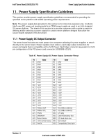
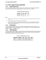
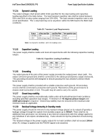
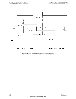
Intel® Server Board S2600GZ/GL TPS Power Supply Specification Guidelines 11.2.4 Dynamic Loading The output voltages shall remain within limits specified for the step loading and capacitive loading specified in the table below. The load transient repetition rate shall be tested between 50Hz and 5kHz at duty cycles ranging from 10%-90%. The load transient repetition rate is only a test specification. The step load may occur anywhere within the MIN load to the MAX load conditions. Table 50. Transient Load Requirements Output +12VSB +12V Step Load Size 1.0A 60% of max load Load Slew Rate 0.25 A/sec 0.25 A/sec Test capacitive Load 20 F 2000 F Note: For dynamic condition +12V min loading is 1A. 11.2.5 Capacitive Loading The power supply shall be stable and meet all requirements with the following capacitive loading ranges. Table 51. Capacitive Loading Conditions Output MIN MAX Units +12VSB 20 3100 F +12V 500 25000 F 11.2.6 Grounding The output ground of the pins of the power supply provides the output power return path. The output connector ground pins shall be connected to the safety ground (power supply enclosure). This grounding should be well designed to ensure passing the max allowed Common Mode Noise levels. The power supply shall be provided with a reliable protective earth ground. All secondary circuits shall be connected to protective earth ground. Resistance of the ground returns to chassis shall not exceed 1.0 m. This path may be used to carry DC current. 11.2.7 Closed loop stability The power supply shall be unconditionally stable under all line/load/transient load conditions including specified capacitive load ranges. A minimum of: 45 degrees phase margin and 10dB-gain margin is required. Closed-loop stability must be ensured at the maximum and minimum loads as applicable. 11.2.8 Residual Voltage Immunity in Standby mode The power supply should be immune to any residual voltage placed on its outputs (Typically a leakage voltage through the system from standby output) up to 500mV. There shall be no additional heat generated, nor stressing of any internal components with this voltage applied to any individual or all outputs simultaneously. It also should not trip the protection circuits during turn on. The residual voltage at the power supply outputs for no load condition shall not exceed 100mV when AC voltage is applied and the PSON# signal is de-asserted. Revision 1.1 105 Intel order number G24881-004
-
 1
1 -
2
-
3
-
4
-
5
-
6
-
7
-
8
-
9
-
10
-
11
-
12
-
13
-
14
-
15
-
16
-
17
-
18
-
19
-
20
-
21
-
22
-
23
-
24
-
25
-
26
-
27
-
28
-
29
-
30
-
31
-
32
-
33
-
34
-
35
-
36
-
37
-
38
-
39
-
40
-
41
-
42
-
43
-
44
-
45
-
46
-
47
-
48
-
49
-
50
-
51
-
52
-
53
-
54
-
55
-
56
-
57
-
58
-
59
-
60
-
61
-
62
-
63
-
64
-
65
-
66
-
67
-
68
-
69
-
70
-
71
-
72
-
73
-
74
-
75
-
76
-
77
-
78
-
79
-
80
-
81
-
82
-
83
-
84
-
85
-
86
-
87
-
88
-
89
-
90
-
91
-
92
-
93
-
94
-
95
-
96
-
97
-
98
-
99
-
100
-
101
-
102
-
103
-
104
-
105
-
106
-
107
-
108
-
109
-
110
-
111
-
112
-
 113
113 -
 114
114 -
 115
115 -
 116
116 -
 117
117 -
 118
118 -
 119
119 -
 120
120 -
 121
121 -
 122
122 -
 123
123 -
124
-
125
-
126
-
127
-
128
-
129
-
130
-
131
-
132
-
133
-
134
-
135
-
136
-
137
-
138
-
139
-
140
-
141
-
142
-
143
-
144
-
145
-
146
-
147
-
148
-
149
-
150
-
151
-
152
-
153
-
154
-
155
-
156
-
157
-
158
-
159
-
160
-
161
-
162
-
163
-
164
-
165
-
166
-
167
-
168
-
169
-
170
-
171
-
172
-
173
-
174
-
175
-
176
-
177
-
178
-
179
-
180
-
181
-
182
-
183
-
184
-
185
-
186
-
187
-
188
-
189
-
190
-
191
-
192
-
193
-
194
-
195
-
196
-
197
-
198
-
199
-
200
-
201
-
202
-
203
-
204
-
205
-
206
-
207
-
208
-
209
-
210
-
211
-
212
-
213
-
214
-
215
-
216
-
217
-
218
-
219
-
220
-
221
-
222
-
223
-
224
-
225
-
226
-
227
-
228
-
229
-
230
-
231
-
232
-
233
-
234
-
235
-
236
-
237
-
238
-
239
-
240
-
241
-
242
-
243
-
244
-
245
-
246
-
247
-
248
-
249
-
250
-
251
-
252
-
253
-
254
-
255
-
256
-
257
-
258
-
259
-
260
-
261
-
262
-
263
-
264
 |
 |
