Intel S2600GZ S2600GZ/GL - Page 9

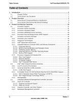
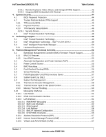
List of s - s2600gl

Page 9 highlights

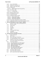
Intel® Server Board S2600GZ/GL TPS List of Figures List of Figures Figure 1. Server Board Component/Features Identification 3 Figure 2. Intel® Light Guided Diagnostic LED Identification 4 Figure 3. Jumper Block Identification 5 Figure 4. Intel® Server Board S2600GZ/S2600GL External I/O Connector Layout 5 Figure 5. Intel® Server Board S2600GZ/GL - Primary Side Keepout Zone 6 Figure 6. Intel® Server Board S2600GZ/GL- Hole and Component Positions 7 Figure 7. Intel® Server Board S2600GZ/GL - Secondary Side Keepout Zone 8 Figure 8. Intel® Server Board S2600GZ/GL- Primary Side Height Restrictions 9 Figure 9. Intel® Server Boards S2600GZ, S2600GL Functional Block Diagram 10 Figure 10. Processor Socket Assembly 11 Figure 11. Processor Socket ILM Variations 12 Figure 12. Integrated Memory Controller Functional Block Diagram 17 Figure 13. Memory Slots Definition 20 Figure 14. Intel® Server Board S2600GZ Memory Slot Layout 21 Figure 15. Intel® Server Board S2600GL Memory Slot Layout 22 Figure 16. Functional Block Diagram of Processor IIO Sub-system 28 Figure 17. Intel® Server Board S2600GZ/GL PCI Layout 29 Figure 18. 1U PCIe riser for Intel® Server Board S2600GZ/GL 30 Figure 19. 2U three PCIe slots riser for Intel® Server Board S2600GZ/GL 30 Figure 20. 2U two PCIe slots riser for Intel® Server Board S2600GZ/GL 31 Figure 21. 2U three PCIx/PCIe slots riser for Intel® Server Board S2600GZ/GL 31 Figure 22. Intel® Server Board S2600GZ/GL External RJ45 NIC Port LED Definition 32 Figure 23. Server Board Layout - I/O Module Connector 33 Figure 24. Server Board Layout - Intel® Integrated RAID Module Option Placement 33 Figure 25. Functional Block Diagram - Chipset Supported Features and Functions 34 Figure 26. Low Profile eUSB SSD Support 35 Figure 27. Intel® RAID C600 Upgrade Key Connector 36 Figure 28. Integrated BMC Block Diagram 39 Figure 29. Integrated BMC Functional Block Diagram 40 Figure 30. Setup Utility - TPM Configuration Screen 47 Figure 31. Fan Speed Control Process 59 Figure 32. Intel® RMM4 Lite Activation Key Installation 76 Figure 33. Intel® RMM4 Dedicated Management NIC Installation 77 Figure 34. Serial-A RJ45 connector pin-out 91 Figure 35. Serial A Configuration Jumper Block Location 92 Figure 36. Reset and Recovery Jumper Block Location 94 Figure 37. On-Board Diagnostic LED Placement 99 Figure 38. Memory Slot Fault LED Locations 99 Figure 39. Turn On/Off Timing (Power Supply Signals 108 Figure 40. Main Screen...112 Revision 1.1 ix Intel order number G24881-004

  • 1
  • 2
  • 3
  • 4
  • 5
  • 6
  • 7
  • 8
  • 9
  • 10
  • 11
  • 12
  • 13
  • 14
  • 15
  • 16
  • 17
  • 18
  • 19
  • 20
  • 21
  • 22
  • 23
  • 24
  • 25
  • 26
  • 27
  • 28
  • 29
  • 30
  • 31
  • 32
  • 33
  • 34
  • 35
  • 36
  • 37
  • 38
  • 39
  • 40
  • 41
  • 42
  • 43
  • 44
  • 45
  • 46
  • 47
  • 48
  • 49
  • 50
  • 51
  • 52
  • 53
  • 54
  • 55
  • 56
  • 57
  • 58
  • 59
  • 60
  • 61
  • 62
  • 63
  • 64
  • 65
  • 66
  • 67
  • 68
  • 69
  • 70
  • 71
  • 72
  • 73
  • 74
  • 75
  • 76
  • 77
  • 78
  • 79
  • 80
  • 81
  • 82
  • 83
  • 84
  • 85
  • 86
  • 87
  • 88
  • 89
  • 90
  • 91
  • 92
  • 93
  • 94
  • 95
  • 96
  • 97
  • 98
  • 99
  • 100
  • 101
  • 102
  • 103
  • 104
  • 105
  • 106
  • 107
  • 108
  • 109
  • 110
  • 111
  • 112
  • 113
  • 114
  • 115
  • 116
  • 117
  • 118
  • 119
  • 120
  • 121
  • 122
  • 123
  • 124
  • 125
  • 126
  • 127
  • 128
  • 129
  • 130
  • 131
  • 132
  • 133
  • 134
  • 135
  • 136
  • 137
  • 138
  • 139
  • 140
  • 141
  • 142
  • 143
  • 144
  • 145
  • 146
  • 147
  • 148
  • 149
  • 150
  • 151
  • 152
  • 153
  • 154
  • 155
  • 156
  • 157
  • 158
  • 159
  • 160
  • 161
  • 162
  • 163
  • 164
  • 165
  • 166
  • 167
  • 168
  • 169
  • 170
  • 171
  • 172
  • 173
  • 174
  • 175
  • 176
  • 177
  • 178
  • 179
  • 180
  • 181
  • 182
  • 183
  • 184
  • 185
  • 186
  • 187
  • 188
  • 189
  • 190
  • 191
  • 192
  • 193
  • 194
  • 195
  • 196
  • 197
  • 198
  • 199
  • 200
  • 201
  • 202
  • 203
  • 204
  • 205
  • 206
  • 207
  • 208
  • 209
  • 210
  • 211
  • 212
  • 213
  • 214
  • 215
  • 216
  • 217
  • 218
  • 219
  • 220
  • 221
  • 222
  • 223
  • 224
  • 225
  • 226
  • 227
  • 228
  • 229
  • 230
  • 231
  • 232
  • 233
  • 234
  • 235
  • 236
  • 237
  • 238
  • 239
  • 240
  • 241
  • 242
  • 243
  • 244
  • 245
  • 246
  • 247
  • 248
  • 249
  • 250
  • 251
  • 252
  • 253
  • 254
  • 255
  • 256
  • 257
  • 258
  • 259
  • 260
  • 261
  • 262
  • 263
  • 264

Intel® Server Board S2600GZ/GL TPS
List of Figures
Revision 1.1
Intel order number G24881-004
ix
List of Figures
Figure 1. Server Board Component/Features Identification
.........................................................
3
Figure 2. Intel
®
Light Guided Diagnostic LED Identification
.........................................................
4
Figure 3. Jumper Block Identification
..........................................................................................
5
Figure 4. Intel
®
Server Board S2600GZ/S2600GL External I/O Connector Layout
......................
5
Figure 5.
Intel
®
Server Board S2600GZ/GL
Primary Side Keepout Zone
.................................
6
Figure 6. Intel
®
Server Board S2600GZ/GL
Hole and Component Positions
.............................
7
Figure 7. Intel
®
Server Board S2600GZ/GL
Secondary Side Keepout Zone
.............................
8
Figure 8. Intel
®
Server Board S2600GZ/GL
Primary Side Height Restrictions
...........................
9
Figure 9. Intel
®
Server Boards S2600GZ, S2600GL Functional Block Diagram
.........................
10
Figure 10. Processor Socket Assembly
.....................................................................................
11
Figure 11. Processor Socket ILM Variations
.............................................................................
12
Figure 12. Integrated Memory Controller Functional Block Diagram
..........................................
17
Figure 13. Memory Slots Definition
...........................................................................................
20
Figure 14. Intel
®
Server Board S2600GZ Memory Slot Layout
..................................................
21
Figure 15. Intel
®
Server Board S2600GL Memory Slot Layout
..................................................
22
Figure 16. Functional Block Diagram of Processor IIO Sub-system
..........................................
28
Figure 17. Intel
®
Server Board S2600GZ/GL PCI Layout
..........................................................
29
Figure 18. 1U PCIe riser for Intel
®
Server Board S2600GZ/GL
..................................................
30
Figure 19. 2U three PCIe slots riser for Intel
®
Server Board S2600GZ/GL
................................
30
Figure 20. 2U two PCIe slots riser for Intel
®
Server Board S2600GZ/GL
...................................
31
Figure 21. 2U three PCIx/PCIe slots riser for Intel
®
Server Board S2600GZ/GL
........................
31
Figure 22. Intel
®
Server Board S2600GZ/GL External RJ45 NIC Port LED Definition
................
32
Figure 23. Server Board Layout - I/O Module Connector
...........................................................
33
Figure 24. Server Board Layout
Intel
®
Integrated RAID Module Option Placement
................
33
Figure 25. Functional Block Diagram - Chipset Supported Features and Functions
..................
34
Figure 26. Low Profile eUSB SSD Support
...............................................................................
35
Figure 27. Intel
®
RAID C600 Upgrade Key Connector
...............................................................
36
Figure 28. Integrated BMC Block Diagram
................................................................................
39
Figure 29. Integrated BMC Functional Block Diagram
...............................................................
40
Figure 30. Setup Utility
TPM Configuration Screen
................................................................
47
Figure 31. Fan Speed Control Process
.....................................................................................
59
Figure 32. Intel
®
RMM4 Lite Activation Key Installation
.............................................................
76
Figure 33. Intel
®
RMM4
Dedicated Management NIC Installation
.............................................
77
Figure 34. Serial-A RJ45 connector pin-out
...............................................................................
91
Figure 35. Serial A Configuration Jumper Block Location
..........................................................
92
Figure 36. Reset and Recovery Jumper Block Location
............................................................
94
Figure 37. On-Board Diagnostic LED Placement
......................................................................
99
Figure 38. Memory Slot Fault LED Locations
............................................................................
99
Figure 39. Turn On/Off Timing (Power Supply Signals)
...........................................................
108
Figure 40. Main Screen
...........................................................................................................
112