Intel S2600CP Technical Product Specification - Page 180
Each DC/DC converter output on PDB has individual OCP protection circuits. The PS+PDB
 |
View all Intel S2600CP manuals
Add to My Manuals
Save this manual to your list of manuals |
Page 180 highlights
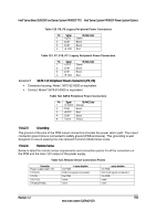
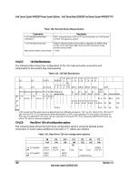
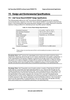
Intel® Server System P4000CP Power System Options Intel® Server Board S2600CP and Server System P4000CP TPS While in Stand-by mode, at no load condition, the residual voltage on each DC/DC converter output does not exceed 100mV. 13.4.3 Protection Circuits The PDB shall shut down all the DC/DC converters on the PDB and the power supply (by PSON) if there is a fault condition on the PDB (OVP or OCP). If the PDB DC/DC converter latches off due to a protection circuit tripping, an AC cycle OFF for 15sec min or a PSON# cycle HIGH for 1sec shall be able to reset the power supply and the PDB. 13.4.3.1 Over-Current Protection (OCP)/240VA Protection Each DC/DC converter output on PDB has individual OCP protection circuits. The PS+PDB combo shall shutdown and latch off after an over current condition occurs. This latch shall be cleared by toggling the PSON# signal or by an AC power interruption. The values are measured at the PDB harness connectors. The DC/DC converters shall not be damaged from repeated power cycling in this condition. Also, the +12V output from the power supply is divided on the PDB into 4 channels and +12V4 is limited to 240VA of power. There are current sensors and limit circuits to shut down the entire PS+PDB combo if the limit is exceeded. The limits are listed in below table. -12V and 5VSB is protected under over current or shorted conditions so that no damage can occur to the power supply. Auto-recovery feature is a requirement on 5VSB rail. Table 134. PDB Over Current Protection Limits/240VA Protection Output Voltage +3.3V +5V +12V1 +12V2 +12V3 Min OCP Trip Limits 27A 27A 91A 76A 18A Max OCP Trip Limits 32A 32A 100A 100A 20A Usage PCIe, Misc PCIe, HDD, Misc CPU1 + memory Fans, Misc HDD and peripherals Connectors P1, P5, P6 P1, P5, P6 P1-P3, P12 P13-P16 P5-P11 13.4.3.2 Over Voltage Protection (OVP) Each DC/DC converter output on PDB have individual OVP protection circuits built in and it shall be locally sensed. The PS+PDB combo shall shutdown and latch off after an over voltage condition occurs. This latch shall be cleared by toggling the PSON# signal or by an AC power interruption. Table 98 contains the over voltage limits. The values are measured at the PDB harness connectors. The voltage shall never exceed the maximum levels when measured at the power pins of the output harness connector during any single point of fail. The voltage shall never trip any lower than the minimum levels when measured at the power pins of the PDB connector. Table 135. Over Voltage Protection (OVP) Limits Output voltage +3.3V +5V -12V +5VSB OVP min (v) 3.9 5.7 -13.3 5.7 OVP max (v) 4.8 6.5 -15.5 6.5 164 Revision 1.2 Intel order number G26942-003
-
 1
1 -
2
-
3
-
4
-
5
-
6
-
7
-
8
-
9
-
10
-
11
-
12
-
13
-
14
-
15
-
16
-
17
-
18
-
19
-
20
-
21
-
22
-
23
-
24
-
25
-
26
-
27
-
28
-
29
-
30
-
31
-
32
-
33
-
34
-
35
-
36
-
37
-
38
-
39
-
40
-
41
-
42
-
43
-
44
-
45
-
46
-
47
-
48
-
49
-
50
-
51
-
52
-
53
-
54
-
55
-
56
-
57
-
58
-
59
-
60
-
61
-
62
-
63
-
64
-
65
-
66
-
67
-
68
-
69
-
70
-
71
-
72
-
73
-
74
-
75
-
76
-
77
-
78
-
79
-
80
-
81
-
82
-
83
-
84
-
85
-
86
-
87
-
88
-
89
-
90
-
91
-
92
-
93
-
94
-
95
-
96
-
97
-
98
-
99
-
100
-
101
-
102
-
103
-
104
-
105
-
106
-
107
-
108
-
109
-
110
-
111
-
112
-
113
-
114
-
115
-
116
-
117
-
118
-
119
-
120
-
121
-
122
-
123
-
124
-
125
-
126
-
127
-
128
-
129
-
130
-
131
-
132
-
133
-
134
-
135
-
136
-
137
-
138
-
139
-
140
-
141
-
142
-
143
-
144
-
145
-
146
-
147
-
148
-
149
-
150
-
151
-
152
-
153
-
154
-
155
-
156
-
157
-
158
-
159
-
160
-
161
-
162
-
163
-
164
-
165
-
166
-
167
-
168
-
169
-
170
-
171
-
172
-
173
-
174
-
 175
175 -
 176
176 -
 177
177 -
 178
178 -
 179
179 -
 180
180 -
 181
181 -
 182
182 -
 183
183 -
 184
184 -
 185
185 -
186
-
187
-
188
-
189
-
190
-
191
-
192
-
193
-
194
-
195
-
196
-
197
-
198
-
199
-
200
-
201
-
202
-
203
-
204
-
205
-
206
-
207
-
208
-
209
-
210
-
211
-
212
-
213
-
214
-
215
-
216
-
217
-
218
-
219
-
220
-
221
-
222
-
223
-
224
-
225
-
226
-
227
-
228
 |
 |